UBI Research, just published ‘AMOLED Manufacturing Process’ report on latest AMOLED process
Recently the smart phone market is led by smart phones that use full screen OLED, and premium TV market is dominated by OLED TVs. In order to realize full screen OLED and UHD resolution large area OLED, different structures and processes have been applied, but it is difficult for the display related companies to grasp them in detail.
UBI Research just published the ‘AMOLED Manufacturing Process’ report, which analyzes the latest processes both for small and medium- sized OLED and large area OLED.
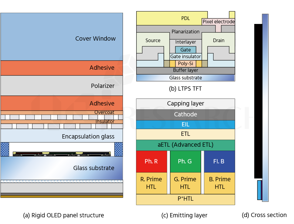
As the report analyzes the structure and manufacturing process by dividing AMOLED into small & medium size and large area with additional description and diagram for the inspection process of small & medium sized AMOLED, it is expected to help to understand the overall structure and core processes of AMOLED.
Chapter 1 of the report covers the overall structure both for small & medium sized OLED and large area OLED, ranging from AMOLED substrates to modules. In Section 2, the double poly (polyimide) process, LTPS TFT & oxide TFT process, pixel process both for OLED & solution processed OLED, process by encapsulation, cell process, and module process are sequentially analyzed. In Chapter 3, the inspection & measurement process of small and medium-sized AMOLED is described with all the list of major equipment. Also, Samsung Display’s pad bending process both for 9-mask LTPS TFT and 13-mask LTPS TFT, and LG Display’s oxide TFT process for large-area OLED are described from Chapter 4. Since the equipment and materials used at each process are analyzed in detail, the report is very helpful to understand easily the latest TFT process.

<Rigid OLED structure, add on type>


