78.6 tons of OLED emitting material demand increased by 5.6% in 2020

According to the 2020 OLED emitting material report published by UBI Research, the demand for emitting materials in 2020 is 78.6 tons, which is 4.2 tons higher than last year’s 74.4 tons. The material used for OLEDs for smartphones and mobile devices is 62.9 tons, and the OLED emitting material for TVs is expected to be 15.7 tons.

In 2019, the total emitting material market was totaled at $ 1.28 billion, and 43% of the total amount was purchased from Samsung Display. It was found that the amount purchased by LG Display was 19.4% and the BOE was 11.6%. LG Display’s purchase of emitting materials accounted for 60.8% of TV use. The order of purchase of emitting materials for mobile devices is in order of Samsung Display, BOE, and LG Display. This is because BOE has a large amount of OLED production for mobiles after Samsung Display.

The OLED panel for TV only produces LG Display, but Samsung Display is pursuing QD-OLED commercialization using blue light emitting material and QD. In addition, although BOE is a white OLED structure similar to LG Display, it is developing a top-emission structure that transmits light in the opposite direction of TFT, and it is expected that three companies will produce OLED panels for TV within a few years, and the emitting material market is expected to increase as well.


The market for emitting materials in 2020 is expected to increase by 7% from 2019 to $ 1.37 billion. Among the emitting materials, green and red hosts are expected to be $ 19.2 billion and $ 19 billion, respectively, and green dopants and P + are expected to be $ 1.37 billion and $ 1.35 billion, respectively.
JDI decided to sell LCD production equipment to a foreign client for 200 million dollars.


JDI announced that it has agreed to sell production equipment at its plant in Hakusan, Ishikawa Prefecture, to a foreign client for 200 million dollars.

The Hakusan plant was JDI’s mainstay factory, producing LCD panels for Apple. The plant was halted in July last year due to sluggish demand. JDI plans to clean up excess facilities that have caused poor performance.

JDI decided to sell LCD production equipment to Apple first and real estate to Sharp later, but negotiations have been delayed due to the effect of the corona virus.

The Hakusan plant was built with Apple’s $ 1.5 billion funds and operated at the end of 2016. But because Apple’s utilization of OLED panels on iPhones has increased in recent years, utilization rate of Hakusan plant has decreased. Moreover, it was a burden for JDI to repay the advances to Apple at the end of February 2020. It is a policy that the funds obtained through the sale of the equipment will be used to repay advances.

Wuhan Tianma 6G OLED line installation delay

The Tianma T4 plant in Wuhan has continued to produce even during the corona period, and the core equipment of the ph2 6G OLED line has already been brought in, but the equipment set-up is delayed due to the inability of overseas equipment companies to enter Wuhan.

In recent, as the number of corona virus spreaders in China, including Wuhan, has declined, equipment set-up is expected to resume from the second quarter, and mass production is expected to start after the third quarter.

The ph2 of Tianma T4 was signed on June 1, 2018, and a total of RMB 14.5 billion was invested. When the Ph2 setup is complete, the Tianma T4 plant will have a total of 35K Capa in 6G.

2020 OLED Manufacturing Equipment Market Forecast

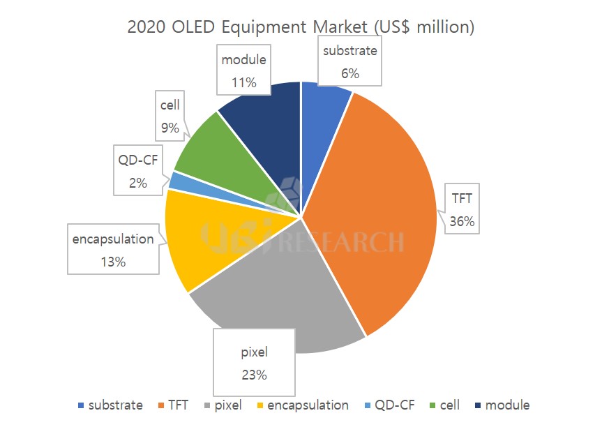
According to UBI Research’s annual equipment market track for 2020, the OLED manufacturing equipment market is expected to reach $ 9.51 billion in 2020. This is an increase of $ 1.2 billion compared to $ 8.31 billion in 2019.

Chinese panel makers have aggressively invested the 6G Flexible OLED line, but due to the high panel price, the adoption of flexible OLED produced in China in the smartphone market has not increased, leading to an oversupply of over 30% worldwide. For this reason, Korea has stopped investing in 6G flexible OLED, and Chinese panel makers are also delaying their investment time slightly.

However, by 2020, Samsung Display’s investment in the 8.5G QD-OLED 30K line began, and the equipment market will remain at the 2019 level.

AP System supplies ELA equipment to Chongqing BOE B12

AP System was selected as the final bidder for BOE’s B12 line ELA (eximer laser annealing) equipment.

ELA is an essential equipment to make low temperature polysilicon (LTPS) TFT for OLED. Eximer laser crystallizes a-Si into polysilicon. It is called LTPS because it makes polysilicon without applying high heat.

In this bid, BOE presented not only equipment quality but also technical competitiveness, easy operation, and maintenance as a supply condition. The AP system met all these requirements and became a final equipment supplier. The official PO has not come out yet.

BOE B12 plans to install eight ELA units. AP System also supplied ELA equipment to BOE’s B7 and B11.

Samsung Display decided to invest 13 trillion won in QD-OLED by 2025

Samsung Display chose QD-OLED as the next generation premium TV. It will also have a big impact on the premium TV market, which is divided between white OLED technology and QLED technology.


Samsung Display announced a new investment and win-win cooperation agreement ceremony at Asan Campus on October 10 and will invest a total of KRW 13 trillion in QD-OLED production facilities and R & D by 2025.


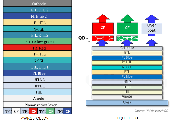
The basic structure of QD-OLED is composed of blue OLED and red and green quantum dot color filters (QD-CF). Blue OLEDs emit blue light, and the red and green QD-CFs convert them to red and green, respectively. QD is also applied to QLEDs because it has the effect of further improving color purity.

Samsung Display will invest 13 trillion won by 2025 to build the world’s first QD display mass production line ‘Q1 Line’ at Asan Campus. The new line will start production in full scale in 2021 with an initial 30,000 sheets (8.5 generations) and will produce a 65-inch or larger ultra-large QD display. To this end, the company plans to convert existing 8G LCD lines into QD OLED lines step by step and gradually expand production capacity by 2025.
 

In addition, in order to accelerate the commercialization of new QD technology, the company plans to shift the existing LCD workforce to QD and hire new QD materials and process development experts. Samsung Display predicted that if investments start in earnest, approximately 81,000 jobs will be created over the next five years.


Lee Dong-hoon, president of Samsung Display, emphasized that “QD, a semiconductor particle that emits light close to natural colors, is the future growth vision of the large display industry.” “We will lead the premium display market with this investment.”

[Press Release] OLED production capacity will increase to double in 2023.

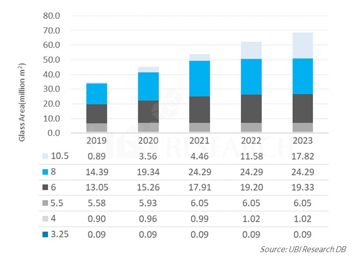
UBI Research has published [2019 OLED Equipment Report] that forecasts the OLED equipment market. According to the report, the total substrate area of display companies in 2019 will be 34.9 million square meters, which will be 68.5 million square meters in 2023 and double after four years.

OLED substrate area growth is attributable to investments made by OLED lines for TVs driven by Samsung Display and LG Display. Currently, OLED manufacturing lines for TVs are 8G lines optimized for 55-inch panel production. However, the demand for premium TVs is shifting from 55-inch OLED TVs to 65-inch TVs. By 2021, the 65-inch OLED TV market will account for more than 40%. In response to these market conditions, LG Display is preparing to invest 10.5G lines in the most efficient production of 65-inch panels. In 2023, the substrate area of a large OLED line is expected to occupy 42% of the total substrate area.

<OLED production capacity by generation>

The substrate area of the 6G line is expected to grow to 13 million square meters this year and to 19.3 million square meters in 2023. Most of this is due to investment by Chinese panel makers. In China, the smartphone market accounts for about 40% of the global market, so Chinese smartphone makers have a very high market share based on the domestic market. Huawei has recently become the world’s second-largest shipper based on its domestic market. Chinese panel makers are boldly adding a 6G flexible OLED line to Chinese smartphone makers, with the Chinese government’s huge support.

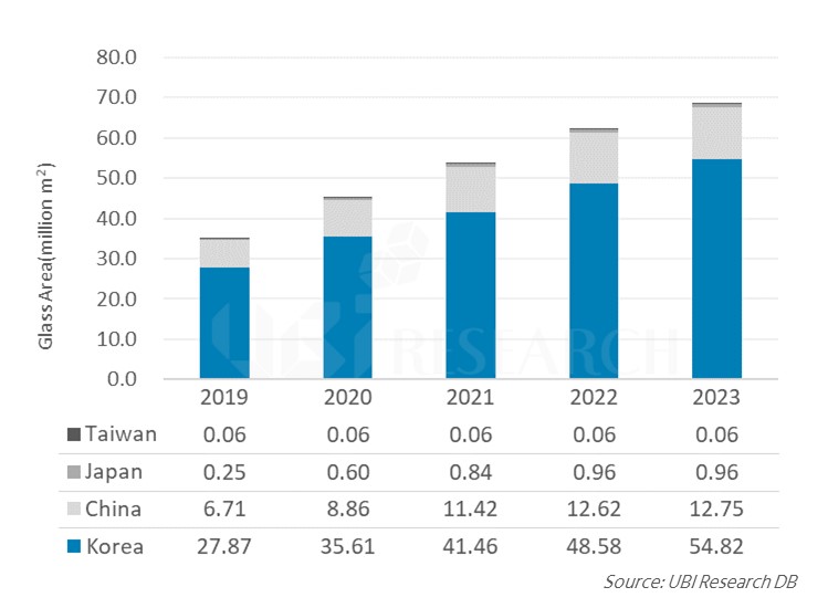
<OLED production capacity by country>

In 2019, Korea’s OLED production capacity (substrate area) will total 27.9 million square meters, accounting for 80% of its total production capacity and expanding to 54.8 million square meters by 2023. The market share will remain at 80% and lead the OLED industry.

Chinese panel makers are expected to stay at around 20% as they are investing only in OLED production lines for mobile device.

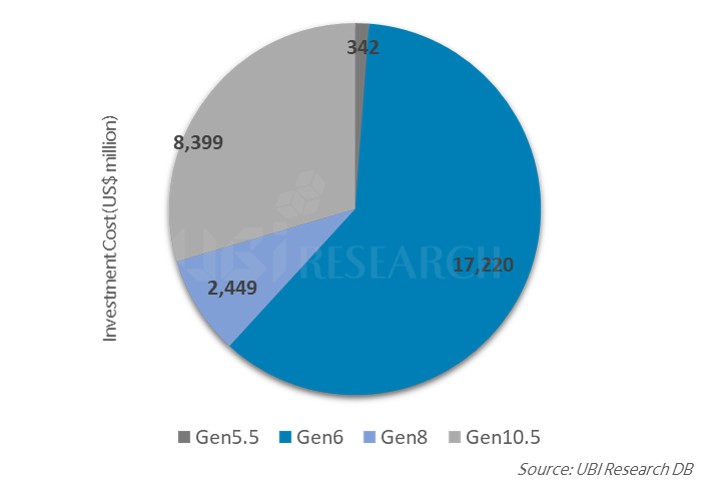
The OLED manufacturing equipment market (excluding logistics equipment) is estimated at $ 28.4 billion for four years from 2019 to 2022 due to investment by Korean and Chinese panel makers. Among them, the sixth-generation equipment market is expected to account for 61% of the total equipment market, at $ 17.2 billion.

<Equipment Market Forecast by Generation (2019 ~ 2022)>

2019 Chinese OLED panel maker equipment order status

As Korean OLED panel makers do not have a lot of investment, the OLED equipment industry is in a low-demand season. When Chinese OLED panel makers confirm the order status of equipment orders in 2019, orders are being made centering on equipment and module line equipment required for new technologies rather than new lines.

In China panel makers BOE and CSOT, some equipment was ordered in March of this year for the development of flexible on-cell touch technology, and Korean equipment makers seem to have received orders from Wonik IPS and Iruja. In addition, since last month, the BOE Chengdu line has begun full-scale mass production and ordering of modular products along with foldable product preparation. Korean equipment makers will also receive equipment orders from BOE and proceed with production.

Starting this month, Visionox Hebei Line, which is set to start full-fledged investment this year, has begun placing orders for long-term delivery equipment and automation equipment. In addition, Wuhan Tianma is making some complementary investments in flexible process equipment, and EDO, Royole, and Truly are expected to invest in the future depending on market conditions.

UBI Research AMOLED process equipment industry report, which is scheduled to be published in May 2019, will be covered in detail in investment situation and equipment supply chain in China panel makers.

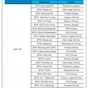
[BOE Chengdu Module Line Order Status]

OLEDON, is to announce belt-plane source deposition technology for manufacturing ultra-high resolution and ultra-area OLED

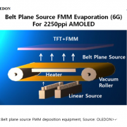
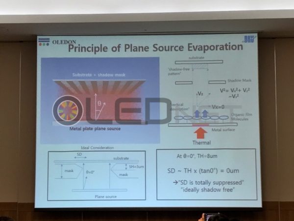
Plane source technology, which was first developed by OLEDON in the world, has the principle of depositing the first organic material on the metal surface and evaporating it upwards to produce fine pattern of 2250 ppi, which is ultrahigh resolution. In this plane source process, three processes such as the first deposition, the plane source inversion, and the second evaporation are necessary, and the number of the high vacuum chambers is increased when the mass production is applied. The belt plane source FMM deposition technology introduced by OLEDON has a concept of carrying out the above processes at a time in one evaporation equipment. This is a continuous plane source supplying deposition technology in which the metal surface is formed in a belt shape.


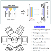
Hwang added, “Using vertical plane source enables smooth deposition process for the 12th generation class area substrate for QD-OLED TV without sagging problem. Vertical belt-plane source evaporation equipment adopts the concept of depositing the substrate in a standing-up position so that the load on the framed glass chuck and the open mask is very low. Thus, easy transportation of the substrate, and uniform deposition process of thin film over a very large area in the static state are possible.” This technology is expected to be applicable not only to the 8th generation but also to the cluster type mass-production evaporator with substrate sizes more than 10 generations in the future.


<Vertical belt plane source evaporator for QD-OLED, Source: OLEDON>

Commenting finally that the company has successfully completed the material denaturation test for blue materials and the blue dopant deposition test, Hwang expected the plane source deposition technology to be applied to both small & medium sized OLED and large area OLED manufacturing in future.

On the other hand, OLEDON holds more than 30 related patents including original patents of plane source and belt plane source evaporator. Also, the company recently filed a patent related to a vertical belt plane source evaporator for mass production.


OLEDON unveils plane source deposition technology for ‘super-gap’ OLED manufacturing.

Attention is growing since OLEDON, a venture company developing OLED deposition equipment, unveiled plane source deposition technology for OLED manufacturing to maintain ‘a superb gap with the competing countries’, at IMID2018, held in COEX, Seoul, Oct. 24, 2018.

Hwang Chang-Hoon, CEO of OLEDON, said, “Korea should actively invest in the development of creative deposition technology to maintain the first place in the current OLED producing countries.” He expects that plane source deposition technology is to be used both for small and medium size OLED and large area OLED manufacturing in future.
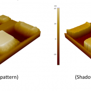
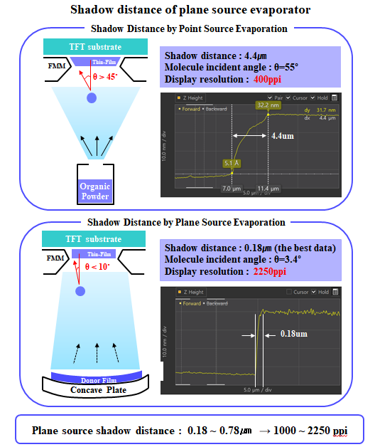
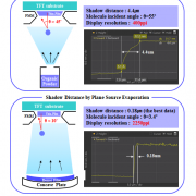
OLEDON is developing the world’s first curved plane source FMM deposition technology, which is an ultra-high-resolution OLED deposition technology capable of manufacturing 2250ppi AMOLED. The shadow distance of fine pattern can be up to 0.18um, enabling 11K high-resolution AMOLED pattern process.


<Existing FMM deposition pattern (left) and plane source FMM deposition pattern (right), Source: OLEDON>

According to Hwang, this process was confirmed with 800 ppi shadow mask, and the emission area of the pattern deposited with plane source was 1.7 times higher than the conventional deposition method.
On the other hand, OLEDON holds the original patent for the FMM deposition technology of plane source, and has recently applied for a patent for vertical plane source deposition for large area OLED TV manufacturing.


<Vertical plane source deposition for OLED TV manufacturing, Source: OLEDON>

OLEDON develops vertical plane source deposition technology for large OLED TV manufacturing

Hwang Chang-Hoon, CEO of OLEDON, which has developed plane-source deposition technology for small & medium-sized OLED and large area OLED, said that it is under development of vertical plane source deposition technology capable of manufacturing ultra-large OLED TVs of 77 inches or larger. Hwang introduced the related technology that it is possible to mass produce OLED TVs of 77 inches or more without the sagging problem of large substrate such as 12th generation (3300 x 4000 mm) substrate when using vertical plane source deposition technology.

According to Hwang, the production yield for 75 inch TVs or larger with the conventional inline type evaporator might be very low due to severe sagging of the substrate and difficult control of many linear sources. To solve this problem, Hwang said that a new 12-generation large-area cluster-type deposition technology is needed, and that vertical plane source deposition technology will be an appropriate alternative.

On the other hand, OLEDON holds the original patents for plane source deposition technology. It also filed a patent related to the curved plane source FMM deposition for high-resolution AMOLED manufacturing, and a patent related to the vertical plane source deposition technology for manufacturing large-area OLED TV.

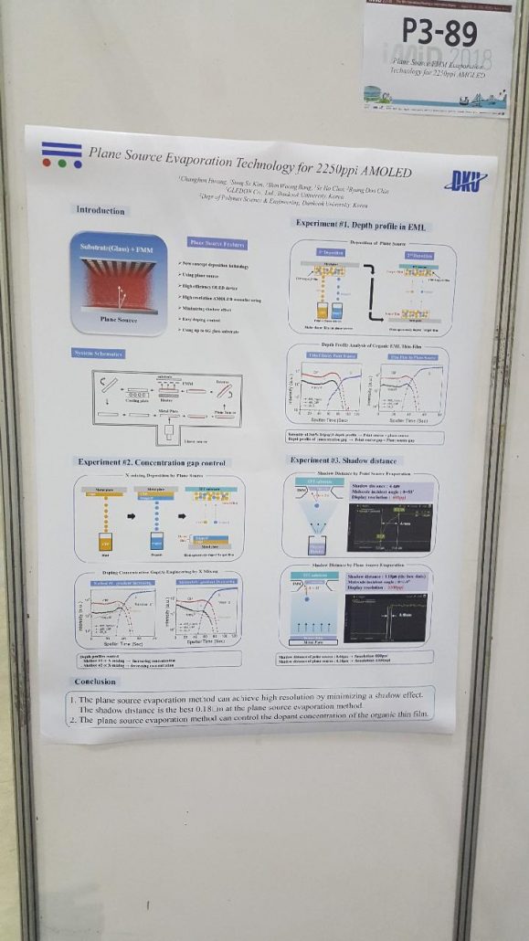
[IMID 2018] OLEDON, developed ‘curved plane source FMM deposition technology’ for 2250ppi AMOLED for the first time in the world

OLEDON is a company which develops plane source deposition technology for high resolution AMOLED manufacturing. Hwang Chang-Hoon, CEO of  OLEDON announced in IMID 2018 that it developed ‘curved plane source FMM deposition technology’ that can be adopted to 2250ppi AMOLED pixels, for the first time in the world.

Conventional linear source FMM deposition technology has a shadow distance of 3um. The available production range is 570ppi AMOLED resolution. On the other hand, the plane source deposition technology already demonstrated in OLEDON can achieve a resolution of 800 to 1200 ppi of AMOLED with a shadow distance of 0.8 to 1.5 μm. Meanwhile, the newly developed ‘curved plane source FMM deposition technology’ is an upgraded technology of the plane source deposition technology which can realize the maximum resolution of AMOLED to 2250ppi with a shadow distance of 0.18 ~ 0.6μm.

The principle is that light is gathered through a concave mirror, a curved surface is applied to the conventional flat plane source, and the light emitting material does not spread, but is precisely deposited at a desired position, thereby reducing the shadow distance.

If this technology is commercialized, it is expected that it can be widely applied not only to mobile devices but also to virtual reality devices.

How much will be the investment cost for 8Generation QD-OLED TV?

In the “2018 OLED Equipment Report” recently published by UBI Research, the required investment cost was analyzed for the QD-OLED that Samsung Display started to develop.

QD-OLED, which is being developed by Samsung Display, is a method of displaying three colors of RGB by separating green and red from the light emitted from blue OLED through QD (quantum dot) material. The light passing through the QD material once again passes through the color filter and displays a richer color.

QD-OLED is similar to the manufacturing method of WDRGB OLED produced by LG Display. First, both companies use oxide TFTs. At WRGB OLED, blue is applied twice and red and green are deposited between them. In contrast, QD-OLED is fabricated by depositing only blue material twice. Both methods use the open mask with an empty center.

For both QD-OLED and WRGB OLED, the color filter manufacturing cost is assumed to be same; however, QD-OLED should be equipped with additional equipment to coat QD materials.

According to the report, it is expected that the investment cost is to be equal because the similar equipment can be used for module, cell, encapsulation and evaporator. Since WRGB OLED is bottom emission type, it is formed together when backplane is formed including TFT. However, QD-OLED adopts top emission method. A color filter is separately formed on the top glass substrate and the QD layer is patterned thereon. Therefore, QD-OLED requires higher investment cost than WRGB OLED.

The report describes that based on 8Generation 26K, the investment cost for QD-OLED is estimated to be US$ 1.1 billion, which is 1.03 times higher than WRGB OLED (US$ 1.07 billion). In contrast, the required investment cost to manufacture OLED by inkjet method, which JOLED is promoting commercialization, is projected as US$ 0.88 billion, which is to be about 80% of QD-OLED.

FlexiGO, developed the durability test equipment capable of accurate evaluation for foldable materials

With the recent announcement that Samsung Electronics and Huawei are aiming to launch smart phones with foldable OLED, folder-type smartphones are drawing attention.

 Display companies are converting glass materials used in the existing substrates and cover windows into plastic materials. Consequently, the durability of plastic materials is becoming an important issue.

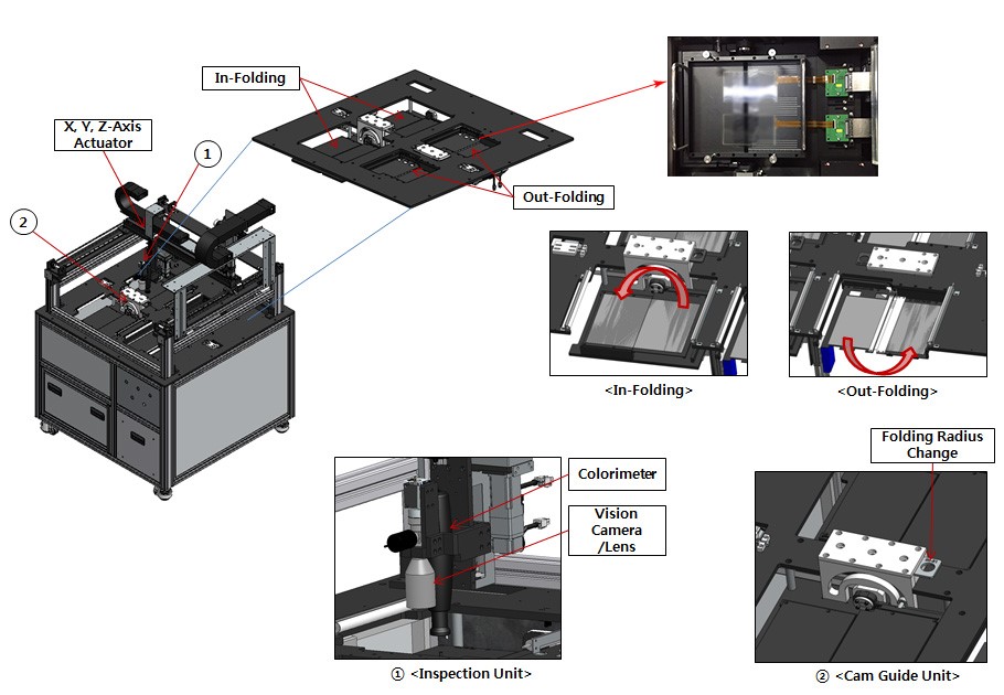
There are various types of durability tests, but the most typical durability inspection is the folding test. The folding test is an experiment that repeatedly bends and unfolds the foldable materials including plastic. Typically, a mechanical device is used for pivoting the rotating plate after fixing some part of the foldable material to the fixed plate and fixing the other remaining part to the rotating plate. However, in the conventional devices, the axis of foldable material is different with that of the rotating plate, the foldable material moves along the rotation path of the rotating plate, not the original rotation path of the material. Thus, there is a possibility that a tensile force acts on the folder material. To solve this problem, FlexiGO recently developed Foldy series, new durability test equipment to test foldable materials.

<FlexiGO’s folding test equipment, Source: flexigo.co.kr>

In addition to the conventional fixed plate and rotating plate, the Foldy series adds a motion controller that supports the fixed plate to move forward and backward for the foldable to be moved only through the original rotation path, so that no other stress is applied to the material. As a sliding device is mounted on the motion controller, the fixed plate moves forward and backward, and the rotating plate performs a rotary motion so that the foldable material can slide on the rotating plate.

The Foldy series includes micro vision, surface profiling, and colorimeter. Foldy-10 and Foldy-100 products can be adopted for the durability test in different test environments. In addition, it is possible to mount an additional inspection system, so it is expected that the accurate durability test of various accurate foldable materials is to be possible.

[iMiD 2017] OLEDON, 2250ppi OLED제조용 면소스 FMM 증착 원리 공개

28일 개최한 iMiD 2017에서 단국대학교의 실험실 벤처 OLEDON사 대표 황창훈 교수는 2250ppi를 구현할 수 있는 면소스 FMM 증착 기술에 대해 발표하였다.

황창훈 교수의 발표에 따르면, OLEDON에서 개발한 면소스 증착 기술은 기존 유기물 증착 방식과 다르다. 면소스 FMM 증착 기술은 유기물을 금속면에 1차로 증착하여 도너 박막을 형성하고 면소스를 만든 후, 이를 재 증발시켜 기판에 유기물 박막을 형성하는 원리이다. 이 기술을 적용하면 유기물은 면증발로 인해 수직성 기체빔을 형성하게 된다. (원천특허:1012061620000 대한민국)

OLEDON사가 개발한 면소스로 유기물을 증착 했을 때의 섀도우 거리는 0.38 um – 0.59 um이다. 이는 4 um의 패턴 사이즈를 가지는 2250ppi 소자를 제작할 수 있는 수준이다.

황창훈 교수는 ‘면소스 증착 기술을 적용하면 유기물 기체의 입사각이 줄어들어 마스크에 의한 섀도우 현상을 획기적으로 줄일 수 있다’고 설명했다. 또한, ‘면소스는 수직성 유기물 기체빔이 완전 제로 입사각을 형성할 수 있어 이론적으로 섀도우 거리가 제로 um도 가능하다’고 덧붙였다.


<OLEDON사가 개발한 면소스 증착 기술 원리>


또한, 이번 발표에서 황창훈 교수는 ‘면소스 증착기술은 고해상도용 섀도우마스크의 제작에도 필수적’이라 강조했다.

현재 양산에 적용중인 리니어 소스 FMM의 경우 섀도우 마스크의 오프닝간 거리는 80um이다. 이로 인해 유기물 기체빔의 입사각은 커질 수 밖에 없어 고밀도 패턴을 가지는 섀도우 마스크 제작이 어려운 실정이다.

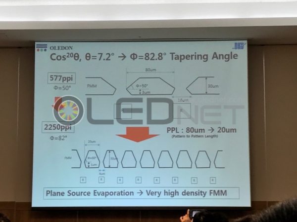
황창훈 교수는 ‘면소스 증착 기술을 이용하면 섀도우 마스크의 테이핑 각도는 80° 수준이다’며 ‘오프닝간 거리를 20 um미만까지 줄일 수 있어 면소스 증착 기술은 리니어 소스가 가지는 마스크 패턴 밀도 문제를 해결할 수 있다’고 설명했다.

OLEDON사는 면소스 증착 기술로 완전 shadow-free 패터닝 조건에 도전하고 있으며, 단국대학교의 진병두교수팀과 공동으로 11K급 마이크로 OLED 소자의 제조가 가능한 면소스 FMM 증착기를 단국대학교내에 개발 설치할 계획이다. (참고:OLEDON사의 홈페이지 www.oledon.co.kr)


<면소스 FMM 증착기술을 사용시 섀도우마스크의 오프닝밀도 변화>


한편, OLEDON사은 양산용 면소스 FMM 증착기에 대한 13건의 등록특허를 보유하고 있다. 최근 연구 결과를 토대로 양산장비 신규특허 7건을 국내출원 하였으며, 3건을 PCT 국제출원 중이다.

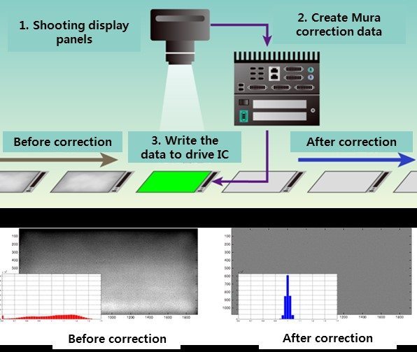
Cybernet, OLED display용 얼룩 보정 IC 개발

일본의 Cybernet system 주식회사는 OLED display용 얼룩 보정 기능 IP를 포함한 display driver IC를 반도체 제조 업체와 공동 개발 했다고 밝혔다.

<OLED와 Driver IC의 구조도 예, 출처 : cybernet.jp>

Cybernet이번 공동 개발을 통해, OLED panel 업체들이 향상 된 얼룩 보정 기능을 쉽게 적용 할 수 있으며, Cybernet이 제공하는 자동 얼룩 보정 장치 FPiS™ series를 동시에 사용함으로써 품질 향상과 수율 개선으로 안정적인 생산을 할 수 있다.” 라며, 이를 바탕으로 시장에 제품 출시가 가속화 될 것으로 기대하고 있다고 밝혔다.

이번에 개발 된 얼룩 보정 기능을 포함한 OLED displaydriver IC 2017 6월부터 범용 IC와 특정 고객을 위한 IC로 판매를 개시 할 예정으로, 상세한 최종 제품 사양과 판매처, 판매시기는 추후에 공지할 예정이라고 밝혔다.

<FPiS를 활용 한 자동 얼룩 보정 장치 시스템 개략도, 출처 : cybernet.jp>

All about OLED in one place, UBI Research, ‘3rd OLED KOREA Conference’ will be held

UBI Research plans to hold the 3rd OLED KOREA Conference with the theme of “Lessons from History and How OLED Can Evolve” at Novotel Ambassador Hotel on Mar. 8 (Wed) to 9 (Thu).

The OLED industry is expected to grow rapidly according to the adaption of full-driven OLED panels by Sony and Apple in 2017 and the competition among panels, equipment, and manufacturing companies can be intensified at the same time. It is necessary to understand and respond strategically to industry trends for successful business under such circumstances. The opportunities to share ideas and concerns each other and close exchanges between Industry-academic institute, panel, materials and equipment companies have been required. UBI Research has prepared a place to freely exchange various information and opinions through the 3rd OLED Korea Conference by reflecting such needs of the industry.

The Korea Conference will be an opportunity to analyze the past trends of OLED which the usage and application range is getting wider and to discuss the successful advancement and strategies to grow the OLED industry for the future. Therefore, it will be a valuable time to practically help the OLED industry.

The Presentation is planned by twenty-four (24) domestic/international experts related to OLED display such as set and panel makers, materials/equipment companies, university/research etc. including UBI Research, Samsung Display, Cynora and CEREBA about followings:

▲Exploring new opportunities with OLED and the preparation, ▲Possible directions and the reasoning for OLED, ▲Lessons from the history and how OLED can be evolved, ▲OLED and its collaboration, investigating the possibilities

We will establish the opportunity to contribute to the growth of the OLED industry based on the sharing of mutual opinions by preparing a networking space between the companies through luncheon during the conference period and breakfast with OLED reception.

Detail information can be found in www.oledkoreaconference.com

AMOLED Manufacturing Equipment Market for Apple, USD 13,000mn for 5 Years…Half of Total 6G Flexible Equipment

Source = UBI Research

Source = UBI Research [2016 OLED Manufacturing Equipment Annual Report]

Hyunjoo Kang / jjoo@olednet.com

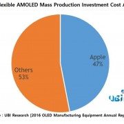
AMOLED manufacturing equipment market for Apple’s use for 5 years, 2016-2020, is expected to reach USD 13,000 million.

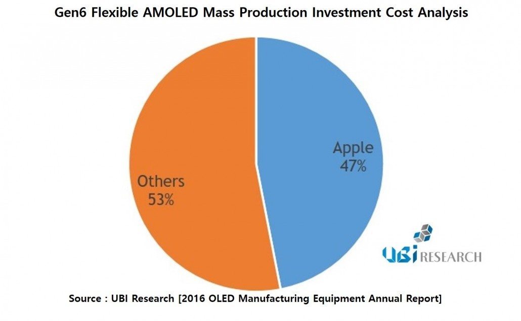
According to 2016 OLED Manufacturing Equipment Annual Report, published on 7 July by UBI Research, the global Gen6 flexible AMOLED manufacturing equipment market is expected to record USD 28,411 million in 2016-2020. 47% of this is for Apple’s use with USD 13,000 million. The figure is if Apple applies flexible panel to some new models of iPhone to be released in 2017, and all new models to be released in 2018.

Apple occupies approximately 15% of the total smartphone sales with over 200 million units per year. As such, it is expected to have great impact on future exible panel market expansion.

In 2021, global flexible AMOLED panel shipment is estimated to exceed 1,000 million units. UBI Research forecasts Apple iPhone’s flexible panel will occupy 20% of the total flexible AMOLED shipment in 2017, and exceed 50% in 2021. UBI Research explains that in order to meet Apple’s flexible AMOLED panel demand, the required panel production capa. is analyzed to be 30K per month in 2017, and total 300K per month in 2021.

Furthermore, panel companies’ mass production line is expanding accordingly, and Samsung Display in particular is expected to invest 30K per year directed to Apple.

UBI Research’s latest report forecasts that the total OLED manufacturing equipment market to record approximately USD 43,927 million in 2016-2020.

Kateeva Promotes Two Key Executives

출처 = Kateeva

출처 = Kateeva

Hyunjoo Kang / jjoo@olednet.com
Kateeva today announced two executive promotions: Conor Madigan, Ph.D. adds Chief Operating Officer (COO) to his current role of President, and Eli Vronsky becomes Chief Product Officer.
Kateeva Chairman and CEO Alain Harrus called Madigan and Vronsky highly accomplished technology experts with strong leadership authority. “Their independent skillsets are extraordinary; together, they’re a powerhouse,” he said. “Nurturing Kateeva from its earliest days, they relentlessly executed on a vision to enable unimaginable display technology innovation. Yet while they disrupted the display industry with a breakthrough production equipment solution, they applied practical business skills along the way, building solid teams, creating best practices, and fostering a corporate culture that guided Kateeva from startup to today’s strong technology company. The Board and I are thrilled to expand their roles.”
Madigan adds global customer satisfaction to his new responsibilities as President and COO. This includes field operations in Korea, China, Taiwan, and Japan. He will continue to manage global marketing and manufacturing, as well as Kateeva’s research and development organization, which incorporates new product development and technology innovations. Also, he’ll lead Kateeva’s expanding Intellectual Property (IP) department – a role he’s held since the company’s inception. This core unit safeguards the ongoing innovations that are empowering Kateeva’s YIELDjet™ products for highest performance in flexible OLED mass-production fabs, and contributing to the development of next-generation products. Madigan co-founded Kateeva in 2008. He reports to Harrus.
As Chief Product Officer, Vronsky owns Kateeva’s product development organization, and leads the company’s high-powered engineering team. An expert in printer technology, Vronsky is chief architect of the fundamental YIELDjet printing system architecture, including the revolutionary process monitoring systems and printing algorithms that helped make Kateeva’s YIELDjet platform the world’s first mass-production-worthy inkjet printer for flexible OLEDs. When it debuted in 2013, the technology provided the breakthrough that liberated display manufacturers from the rigid constraints of glass substrates, to spark the flexible OLED revolution. Much of Kateeva’s highest-value customer-enabling IP surrounds Vronsky’s inventions. Today, he’s applying the same innovation to Kateeva’s new product initiatives. He joined Kateeva in 2008. Previously, he was Executive Vice President of Product Development. He reports to Madigan.