Merck’s Blue Ink Material Lifetime Announced 65% Improvement Year-over-Year.

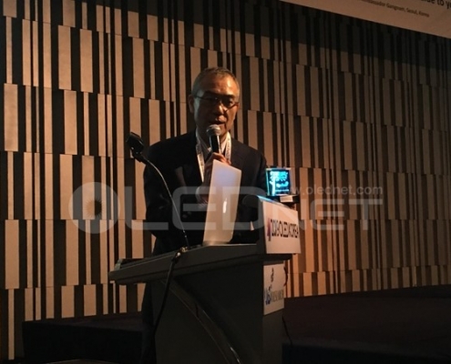
At ‘Display Insight 2021’ held online on November 4th, ‘Joachim Kaiser’, global application manager of Merck, presented ‘Our OLED solutions – livilux®’. When presenting the ink portion of livilux’s OLED materials, Kaiser noted that “Inkjet printing is the only technology that combines RGB parallel pixel layout with scalability for large display sizes”.

Kaiser announced “Maximizing the performance of IJP devices requires a thorough understanding and optimization of state-of-the-art OLED materials, ink formulations optimized for each application, and the entire device stack” and “Merck can get a lot of benefits from IJP performance improvement from its experience in developing materials for deposition”.

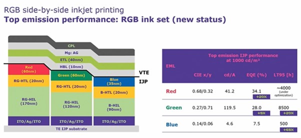
Comparing the performance announced by Merck last year and this year, the luminous efficiency (cd/A) of red increased by 46% compared to the previous year, green by 10%, and blue did not change. External quantum efficiency (EQE) was 34.1%, increased by 20% for red, and 28%, increased by 5% for green, and there was no change in blue like the luminous efficiency. In terms of lifespan, 20% for green and 65% for blue were greatly improved. The lifespan of the red is 4,000 hours based on LT95 (last year’s red’s lifespan was 8,300 hours based on LT95), and it is being optimized to increase the lifetime reduced by improving efficiency.

Kaiser emphasized, “At Merck, we are constantly working to provide solutions to the problems of OLED panel design, such as improving the efficiency of Blue OLED, a new kind of emitter, and RGB side-by-side printing technology.”

[GLOBAL TECH KOREA 2021] Solus Advanced Materials ‘Expansion of new businesses other than light emitting materials such as high refractive filler and TFE’

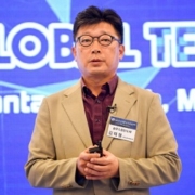
At ‘GLOBAL TECH KOREA 2021’ held in September 2021, Taehyung Kim, Head of Electronic Materials Business Division, Solus Advanced Materials made a presentation under the theme of ‘Solus’ Giant Step To Lead OLED Materials Technology’.

Solus Advanced Materials has monopolized the HBL market for over 8 years as a domestic display material specialist. Director Kim of Solus Advanced Materials said, “During the development of HBL, we also developed ETL with similar chemical structure and important compatibility with HBL. The performance is evaluated as equal to or higher than that of other companies’ top performance, and it will be able to enter the market soon.”

Director Kim said, “Originally, we mainly developed ETL or HBL related to electronics, but it was difficult to develop from the perspective of the overall device, so we developed HTL related to hall.” In addition “The development of HTL was completed about two years ago through joint development with LG Display, and it was approved for large panel use in May” he said. He also said, “The panel supply is gradually increasing and will be expanded to the Guangzhou line by next year.”, “HTL is structurally related to g-prime for mobile, so it is expected that it can be expanded to g-prime on the mobile side,” he said.

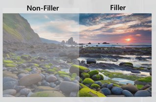
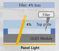
Solus Advanced Materials is developing not only light-emitting materials, but also high-refractive fillers and TFEs. Director Kim said, “The mass production of fillers will be visible from this year. There are various materials such as epoxy, urethane, and acrylic type, and we plan to mass-produce the refractive index and viscosity control according to customer specifications.”

In the TFE sector, General Manager Kim said, “The permittivity of TFE currently used in the market is 3.0 or higher, and we received a request to lower the permittivity of the monomer by 30% or more to increase touch sensitivity two years ago and have been developing it. “The permittivity of the TFE monomer being developed by Solus is down to 20%, and the UV CUT function has achieved a specification of less than 5% at around 400 nanometers, and it is being promoted and tested by customers.”

Solus Advanced Materials is currently expanding its OLED-related businesses to various OLED-related luminescent materials such as HBL, ETL, and HTL, as well as high-refractive materials and TFE monomers. It is noteworthy in which areas these various business groups can shine in the future


Material Science Co., Ltd. develops high-purity blue light-emitting material with a half width of 11 nm

In OLEDs which are currently leading the display industry for mobile devices and TVs, blue material is still using fluorescent material unlike red and green.

Currently, a lot of light emitting material companies are trying to improve the efficiency, lifespan, and color purity of blue light emitting materials, also next-generation materials such as phosphorescence, TADF, and hyper-fluorescence as well as actively developing luminous efficiency by controlling emission wavelengths.

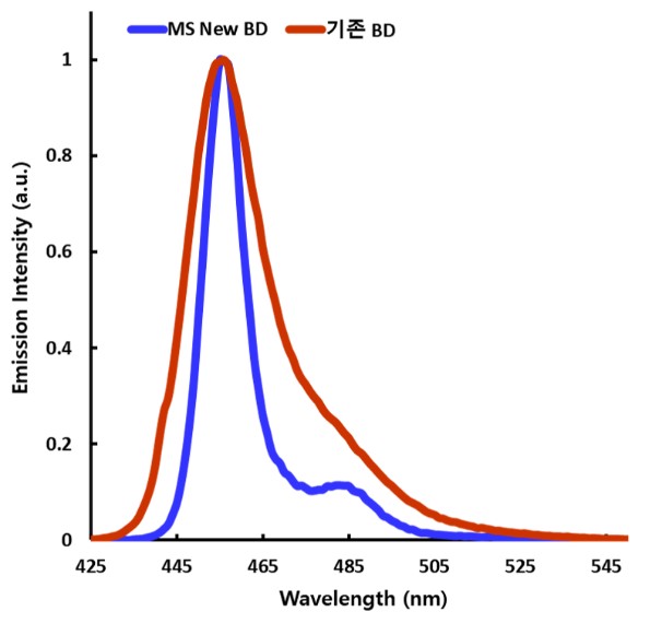
Material Science (hereinafter referred to as MS), a Korean company that has been developing blue light emitting materials since 2015, has recently focused on realizing high color purity and successfully developed high color purity blue light emitting materials with a light emission wavelength of 460 nm and a half width of 11 nm. Considering that the emission wavelength of the currently commercially available blue material is about 20 nm, the blue material of MS is expected to receive great attention.

The full width at half maximum (FWHM) is an expression of the extent of function given by the difference between the two extreme values of the independent variable at which the dependent variable is equal to half of its maximum value.


and the narrower the half width, the higher the purity.

A typical example is Samsung Electronics’ QLED TV, which has significantly improved color reproduction by applying a QD sheet to the LCD back light.

The blue light emitting material developed by MS is expected to be applicable not only to fluorescent materials but also to hyper-fluorescence, which is attracting attention as a next-generation blue material according to emission wavelength control.

<Comparison of the half width of the existing blue dopant with the half width of the blue dopant developed by MS, Source: Materials Science>

Deuterium substitution blue, will be next generation blue materials?

Fluorescent blue emitting material is the only fluorescent material used in small and medium-sized OLEDs and large-area OLEDs.

Development of next generation emitting materials such as TADF and hyper-fluorescence is also in progress, but deuterium substitution technology has got attention since it is adopted to Samsung Galaxy S20.

Deuterium substitution technology is to replace hydrogen with deuterium in a compound combined with existing hydrogen, and each company has a difference in substituting the compound before or after synthesis or substituting the whole. Representative development companies for deuterium substitution include Idemitsu Kosan, DuPont, SFC, and JNC.

As related patents, compounds substituted with deuterium with an atomic mass of deuterium that is twice as high as hydrogen have lower zero-energy and lower vibrational energy than those combined with hydrogen, resulting in lower ground-state energy and weaker intermolecular interactions, resulting in a thin film in an amorphous state. It is effective in improving the life of OLED.

It is expected that the OLED device to which the deuterium-substituted compound is applied can improve the lifetime by more than 20% compared to the previous one.

Molecular Glasses Receives U.S. Patent 10,593,886 For Improved OLED Device Lifetime

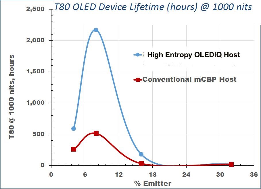
The U.S. Patent Office has awarded patent number U.S. 10,593,886 to Molecular Glasses, Inc. for “OLED Devices with Improved Lifetime Using Non-Crystallizable Molecular Glass Mixture Hosts”

<Improved OLED device lifetime using OLEDIQ™, Source: molecularglasses.com>

The present invention provides an OLED multilayer electroluminescent device that includes a cathode, an anode, a light-emitting layer (LEL) disposed there between, and charge-transporting layers disposed between (A) the cathode and the light-emitting layer, (B) the anode and the light-emitting layer, or (C) both (A) and (B). The light-emitting layer (LEL) includes a host material and an emitter. The host material includes a high-entropy non-crystallizable molecular glass mixture, which includes hole-transporting capabilities, electron-transporting capabilities, or ambipolar capabilities. The ambipolar capabilities include hole-transporting capabilities and electron-transporting capabilities.

According to Mike Molaire, Molecular Glasses’ CEO and Founder, “OLEDIQ™ materials are amorphous, soluble small molecules that are non-crystallizable, which prevents aggregation of dopant emitters. This means OLEDIQ™ produces significant improvements in OLED lifetime and high reliability. This is an ideal platform for high-efficiency, long-lasting blue OLED. OLEDIQ™ materials can be used for both the vacuum-thermal deposition production process, as well as inkjet printing without any modification”.

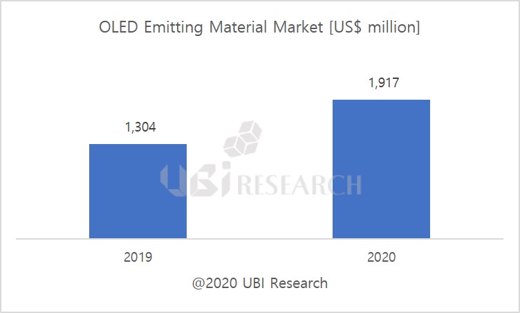
The OLED emitting material market will grow to $ 1.9 billion by 2020

UBI Research(www.ubiresearch.com), a company specializing in OLED market research, predicted that the market for OLED emitting materials for 2020 will rapidly grow to $ 1.9 billion.

According to the OLED emitting material market track published by UBI Research every quarter, the emitting material market in 2019 was $ 1.304 billion, up 39.2% from 2018’s $ 0.937 billion market.

The reason for the growth of the emitting market in 2019 is proportional to the growth of the OLED panel market for smartphones. This is because OLED shipments for smartphones in 2018 were 407 million units, but growth was 16% in 2019 at 474 million units. (Source: UBI Research 2020 OLED Display Market Track).

The reason why the emitting material market growth is greater than that of the panel market is that 6G flexible OLED factories of Chinese panel makers have started operation. The production amount is still small, but the yield is low, so the input of the substrate is twice the amount of production, so the consumption of emitting materials is very high. In addition, it is one of the reasons that the market for emitting materials has grown due to the small purchase volume compared to Samsung Display.

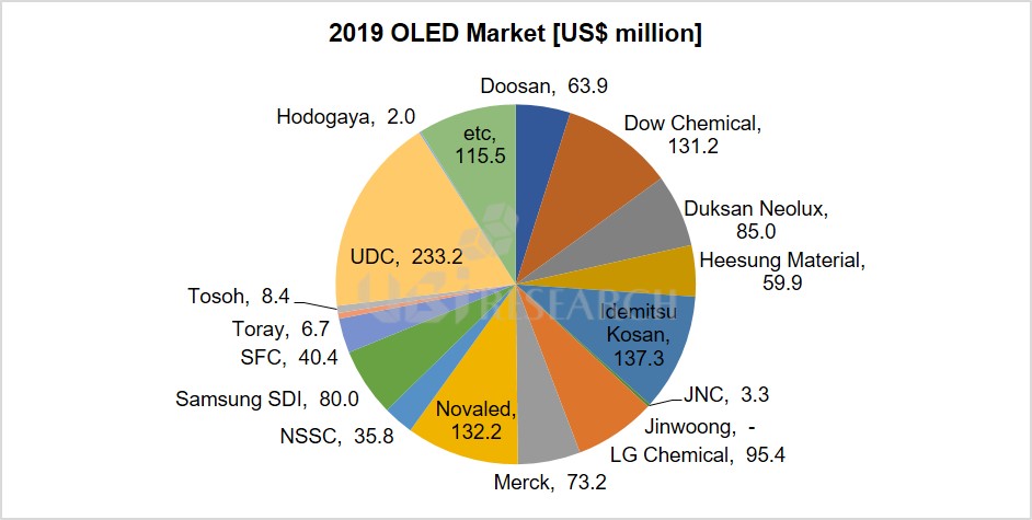
As a result of counting sales by emitting materials companies in 2019, UDC accounted for $ 233 million, accounting for 17.9% of total sales, and Samsung SDI accounted for $ 212 million (including Novaled sales), accounting for 16.2%.

In 2020, both panel makers’ capacity and utilization rate are expected to increase, and consumption of emitting materials is also expected to increase.

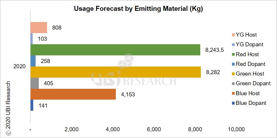
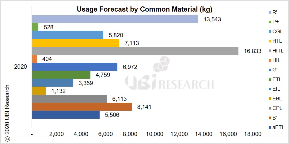
The total consumption of emitting materials in 2019 was 73 tons, but it is expected to increase to 102 tons in 2020.

Expected consumption for each material is 16.9 tons for HITL materials and 4.15 tons for blue host materials. Blue host and dopant materials are expected to increase rapidly from 2021 when Samsung Display starts mass production of QD-OLED.

Canon enters OLED materials business

Canon is considering the OLED materials business as the adoption of OLED panels such as smartphones and TVs is spreading. OLED panels are used in electronic finders in Canon’s mirrorless cameras.

Although no specific production date has been announced, the company will focus on research and development, group companies in Fukui Prefecture, and Fukui Canon.

Canon Tokki, the No. 1 OLED evaporator market share, is a subsidiary.

Canon is developing TADF luminescent materials as Cu-complex compounds. (Japanese Patent JP2011213643A)

2019 Solution Process OLED Annual Report

Solution process using inkjet OLED (sol OLED) has been developed mainly as a large OLED panel for TV, but recently began to attract attention in the monitor display market.

The evaporation method with FMM that produces OLED for smartphones has a bending phenomenon of FMM. Thus, the substrate is used by dividing into two or four. Since smartphone-sized FMMs are used by attaching 10 to 15 sheets to the mask frame, the profitability is very low due to the small number of cells in the production of 20-inch or larger monitors.

In comparison, sol OLED is a highly productive method because OLED can be manufactured from the original substrate regardless of substrate size and display size.

If the 27-inch and 32-inch OLED panels, which are mainly used as gaming monitors, are produced by the FMM method, four can be produced. But sol OLEDs do not divide the substrate, so the 27-inch can make eight, and the 32-inch can make six.

Therefore, in the future, OLED manufacturing technology is expected to be used in combination of three technologies depending on the application and size. Smartphone OLEDs are expected to be divided into FMM and evaporation methods, large OLED panel manufacturing for TVs with open mask and evaporation technology, and sol OLED technology for monitors larger than 25 inches.

There are three types of premium monitor market, LCD, RGB OLED, and sol OLED, but the premium OLED monitor market will be replaced by sol OLED. If 6G-class inkjet lines are invested in large quantities, sol OLED will become the flagship product in the mid-priced monitor market.

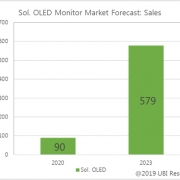
The solution process OLED annual report, published by UBI Research (www.ubiresearch.com), expects to create a market of $ 579 million by 2023. This amount represents 85.3% of the OLED monitor market by 2023.

[Press Release] Opening Ceremony of new Novaled Headquarters(Dresden, Germany, June 2019)

Investment of 30 million Euros in Novaled Headquarters with state-of-the-art R & D center for OLED cutting-edge technology in Dresden, Germany

After 2 years of construction Novaled GmbH opened its new headquarters in Dresden on June, 12th together with long-standing business partners and supporters. Besides representatives of Samsung SDI, the Prime Minister of Saxony, Michael Kretschmer, and the First Mayor of the city of Dresden, Dirk Hilbert, participated in the event.

Core of the 10,200 m² premises in the northern part of the city is a 110 m long R & D center with chemistry laboratories as well as cleanrooms of class ISO5 and ISO7 equipped at highest standards. The new location is an improvement all along the line. Additional space in cleanrooms allowed for investments in cluster tools. This increased the OLED processing capacity by around 40%. The generously planned chemistry laboratories with state-of-the-art equipment and proprietary analytics are a true quantum leap in the development of new materials for high-performance OLEDs.

Novaled is currently the only supplier of organic dopants for OLED display mass production in the industry. Know-how and materials from Dresden enhance therefore most high end smartphones, TVs and smart watches, equipped with OLED displays.

“State-of-the-art cleanrooms, three times more lab space and entirely new facilities offer the best conditions for innovation,” said Novaled CEO Gerd Günther. The company started back in 2003 with five key patents concerning organic electronics. Meanwhile there are nearly 1,000 Novaled patents granted or pending. “Our technologies and materials are established as an industry standard in the OLED display field,” said Gerd Günther. “Novaleds revenues clearly show that we are growing even stronger than the market.”

In addition to the construction of a new technical center, the former mill of the army bakery was extensively renovated and Novaled employees get to work there in loft-like, bright offices. A green outdoor area offers an attractive environment for meetings and relaxation. During the opening ceremony, a birch tree was planted by Novaled CEO Gerd Günther, Samsung SDI Executive Vice President Dr. Hyuk Chang , the Prime Minister of Saxony, Michael Kretschmer and the First Mayor of Dresden, Dirk Hilbert and. “The birch is a known symbol for light and a new beginning, representing what we do in our new premises,” explained Gerd Günther.

About Novaled

Novaled GmbH is a leader in the research, development and commercialization of technologies and materials that enhance the performance of OLEDs (organic light-emitting diodes) and other organic electronics. Novaled offers OLED product manufacturers a unique combination of proprietary technology, materials and expertise, and is currently the only company in the OLED industry licensing and selling organic conductivity doping technology and materials for use in the commercial mass production of display products. Novaled has developed strategic partnerships with key OLED innovators and producers throughout the world and, with a broad portfolio of more than 980 patents granted or pending, has a strong IP position in OLED technologies, structures and materials. Novaled is headquartered in Dresden with some 135 staff and offices in Asia. Since end of 2013 Novaled belongs to Samsung. www.novaled.com


About OLEDs

OLEDs (organic light-emitting diodes) are solid-state devices composed of multiple thin layers of organic materials often only a few nanometers thick that emit diffuse light when electricity is applied to them. Because they are an area light source, OLEDs are a key part of fulfilling the dream of the rapidly growing flat panel display market: paper-thin, highly-efficient displays with brilliant colors and excellent design flexibility. OLEDs may also lead to innovative decorative lighting applications and personalized environments. www.novaled.com/oleds/

OLED emitting materials market to grow to $ 1.71 billion in 2019

OLED light emitting materials market is gradually increasing as Chinese companies enter OLED panel market led by Samsung Display and LG Display.

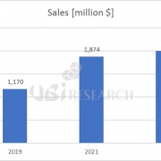
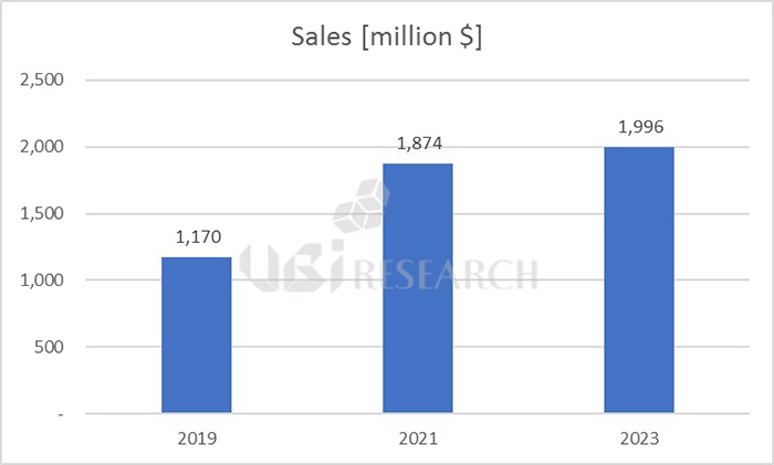
The 2019 OLED emitting material report, published by UBI Research, predicts that the emitting material market in 2019 will reach $ 1.17 billion. 2021 and 2023 are expected to grow to $ 1.87 billion and $ 2.0 billion, respectively.

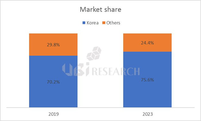
The size of light emitting materials consumed by Korean companies will account for 70.2% in 2019 ($ 0.82 billion), and its share will increase to 75.6% in 2023.

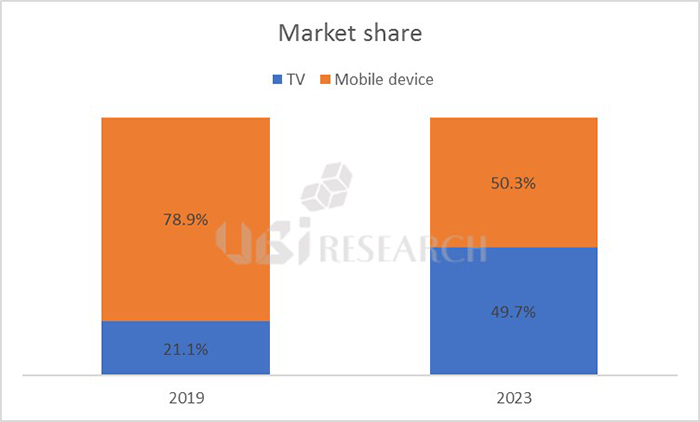
Korea’s emitting material market is growing because the consumption of OLED materials for TVs is soaring. In 2019, 21.1% of light emitting materials for TVs are expected to increase to 49.7% in 2023.

2019 OLED KOREA] Unveiled the latest performance of TADF and Hyperfluorescence, the next generation blue light emitting material

CYNORA and Kyulux have unveiled the latest blue TADF performance and blue hyperfluorescence performance at the 2019 OLED KOREA, which is being held at Novotel Hotel in Gangnam from March 6 to 7, 2019.


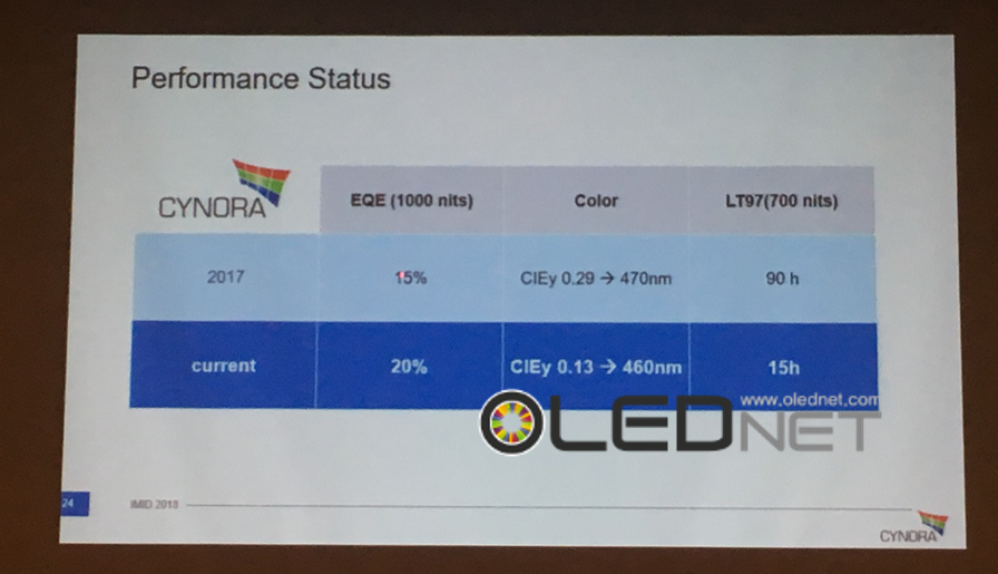
Andreas Haldi, chief marketing officer at CYNORA, revealed that the color coordinates of the blue TADF emitter developed by them are 0.13, 20% for EQE and 5 hours for LT95 @ 1,200 nit.

He said, CYNORA in developing deep blue TADF in earnest from 2018, and will find green and red TADF after blue TADF development.


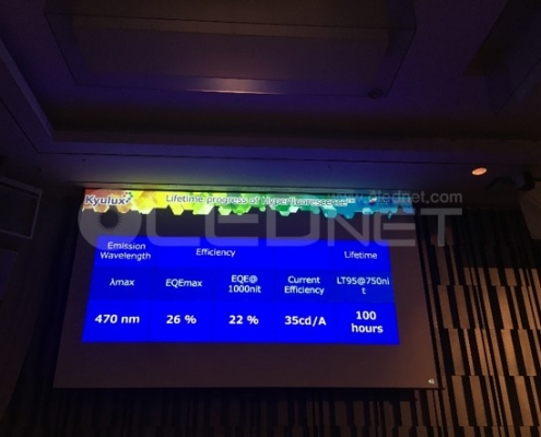
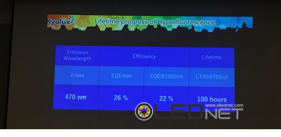
“The maximum EQE of blue hyperfluorescence is 26%, the EQE at 1,000 nit is 22% and the lifetime (LT95 @ 750 nit) is 100 hours,” said Junji Adachi, CEO of Kyulux.

Junji Adachi, CEO, also introduced applications using blue hyperfluorescence and emphasized the potential of hyperfluorescence as a next-generation luminous material.

What is the cost of OLED materials for the Galaxy F?

What will be the price of foldable phone Galaxy F, which is expected to be on the market this year, is a concern for people around the world. Samsung Display is the only company that can mass-produce Foldable OLEDs with in-folding type used by Galaxy F.

Galaxy F with 7.29-inch OLED is a digital convergence product that can simultaneously target the smartphone and tablet PC market. The initial sale price will be around $ 2,000, and the estimated sales volume is about 1 million units this year.

The OLED industry is interested in how much the Galaxy F’s foldable OLED panels (including modules) will cost.

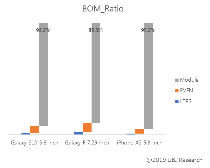
According to UBI Research’s material cost analysis data, Samsung Display’s foldable OLED material cost is 2.04 times higher than the Galaxy S10 5.8 inch. This is because the display area has increased, and the yield has been reduced.

Galaxy F, Galaxy S10, and iPhone XS’s flexible OLED material cost analysis shows that the module cost of iPhone XS is the highest at 95.2%, Galaxy S10 at 92.2% and Galaxy F at 89.3%.

[28TH FINETECH JAPAN] JDI and JOLED, announced Strengthening Cooperation for Mid-sized OLED Market

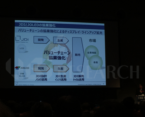
At the 28th FINETECH JAPAN held in Tokyo, Japan from December 5 to 7, 2018, JDI and JOLED announced that they would intensify their cooperation in order to target the middle-sized OLED market.

JDI announced that it will actively promote JOLED’s solution process OLED to medium-sized OLED markets such as industrial display markets or automotive display markets through its own design know-how, production infrastructure, and sales channels,.

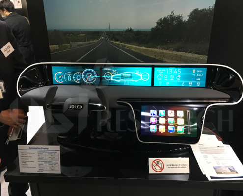
In particular, JDI announced that it will provide new value to next-generation automotive fields along with JOLED such as support for safety such as electronic mirrors and displays for A/B pillars, new interface functions, movie appreciation using 4-8K displays, and the displays that are harmonized with interior design such as curved surfaces and big screens.

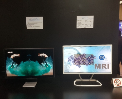
JDI and JOLED also shared booths for exhibition. JOLED introduced 21.6-inch FHD OLED monitors for e-sports and medical applications. In addition, it introduced a number of medium-sized OLEDs such as 12.3-inch HD OLED for automobiles, 12.2-inch FHD flexible OLED, 27-inch 4K OLED for home interior, and 21.6-inch 4K flexible OLED with cylindrical form. It also showcased large OLEDs such as 54.6 inch 4K OLED.

On the other hand, JOLED announced in July, 2018 that it would open its Nomi office for mass production of solution process OLED. Based on 5.5 generation glass substrates, Nomi has production capacity of 20,000 glass substrates per month and plans to mass-produce in 2020.

JOLED, introduced many inkjet OLED technologies

This was the first time for JOLED to demonstrate its products and technologies at FINETECH Japan 2018.

JOLED, which received the inkjet OLED technology from Panasonic and is doing OLED panel business, has been selling medical monitors since early this year. Next year, Asus is also scheduled to sell inkjet OLED TVs made by JOLED.

Its exhibited products include medical OLED monitor, OLED monitor for games, automotive OLED and 3 kinds of OLED TVs.


JOLED’s Inkjet OLEDs have a peak intensity of 350 nit. In case of full white, it is 140 nits, but has sufficient brightness for monitor applications.

JOLED will build mass production lines next year to produce OLEDs for 20-inch monitors and TVs as a full-scale. It also plans to start OLED business for automobiles after 2020.

JOLED is the only company producing OLED panels manufactured by inkjet technology. JOLED is also promoting the license business by providing this technology to Chinese, Japanese and Taiwanese panel makers.

[ICEL 2018] TADF attracts attention as next generation emitting material

In addition to monitors and virtual reality devices, OLED is gradually expanding its domain beyond smartphones and TVs, inclusive of the application of side-mirror OLED in automobiles. As new OLED applications are increased in various environments, it is essential to develop technologies to satisfy users.

In ICEL 2018, which is being held at Jeju International Convention Center from October 15th, many presenters and attendants emphasized that material development is essential to improve the performance of OLED as the OLED market grows more. As an alternative material, TADF (Thermally Activated Delayed Fluorescence) is mentioned.

First, Hwang Seok-Hwan, chief researcher in Samsung Display said that TADF is to be a good resolution as one of emitting materials for new deposition process, referring to the continued growth of OLED panel and material market.


Hwang said that the efficiency of fluorescent Blue is almost saturated, so 100% luminance efficiency can be obtained theoretically by applying TADF with the advantages of not using expensive rare earth metals. He added that improvement of material stability, improvement of color purity by using boron material, development of host having high triplet energy need to be superseded.


Also, CYNORA, a leading TADF developing company, disclosed the performance of dark blue TADF developed so far.

CYNORA said that the luminance efficiency and color purity of dark blue TADF reached the level that the related companies required, and that its current goal is to develop the technology to improve lifetime. In addition, based on this know-how, the company will quickly develop green and red TADF, and now green TADF has been delivered to several customers as a sample.


Merck confirmed that TADF is the most powerful luminescent material to replace fluorescent Blue at its presentation together with a poster about TADF.

OLED companies and research institutes are focusing attention on whether blue TADF can quickly enter OLED market and upgrade OLED performance further.


[ICEL 2018] What are the future challenges for LG Display to improve OLED TV performance?

At ICEL 2018, held at Jeju International Convention Center from Oct. 15, Soo-Young Yoon, Vice President and Head of LG Display Laboratory, presented the challenges for the OLED TV performance improvement and price reduction


Yoon said “In 2018, the future prospects of OLED TVs have changed more positively compared to that in 2016. In 2013, only LG Electronics was an OLED TV set maker. The number of OLED TV set makers has steadily increased; ten in 2016, and fifteen in 2018. Many TV set makers are choosing OLED. ”

He added that although OLED TV is on the track of success with lots of improvement, it has to be further developed. The challenge is the improvement for high brightness, color reproduction rate and with the development of 8K resolution. Also he mentioned that the price reduction is to be necessary.


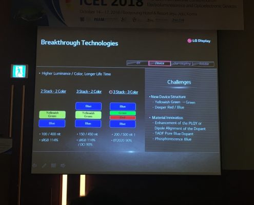
Yoon explained that the development of components such as driver IC and controller is an important task to develop 8K OLED TV. In order to improve the brightness, color reproducibility, and lifespan, TADF and phosphorescent Blue are to be good alternatives for improving the RGB emitting materials. The enhancement of out-coupling is also important.

In addition, he referred to the solution processed OLED as a technology, to compete against LCD TV price, with the necessity of developing inkjet equipment, process, and soluble materials. For this, it is required to develop the ink jet equipment and shorten the process time for mass production, but the performance and reliability of the soluble materials will be more important.
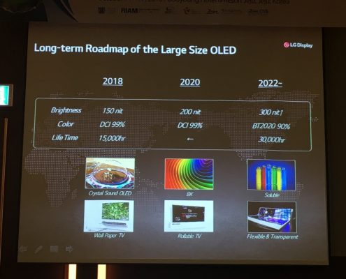
Finally, he commented that the company will focus on 8K OLED TV and rollable OLED TV with the improvement of brightness until 2020. After 2022, the company will develop the OLED TV which has an enhanced brightness of 300 nits or more, a color gamut that satisfies BT.2020, and a lifespan of more than 30,000 hours.


CYNORA announced that it has extended its joint development agreement for TADF commercialization with LG Display.

TADF developer CYNORA has announced that it has extended its joint-development agreement with LG Display. The two companies have been co-developing deep-blue TADF OLED emitters for two years, and have now decided to continue the cooperation towards the commercialization of TADF emitters in OLED displays.

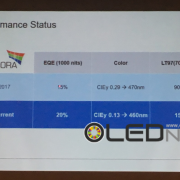
The performance of CYNORA’s latest deep-blue material was presented at IMID 2018 held in August of the year. Among the performance introduced, the CIEy is 0.13, the EQE is 20% based on 1000 nits, and the LT97 is 15 hours at 700 nits.

CYNORA CEO Gildas Sorin commented, “Currently, CYNORA focuses on the development of deep blue TADFs for OLED TVs. Through the accumulated know-how to develop deep blue TADF, it also has plans to develop a light blue TADF for lighting applications and a green TADF for displays.”

[IMID 2018] Can Blue TADF and Hyperfluorescence meet both efficiency and lifetime?

At IMID 2018 in Busan, BEXCO on August 31, Junji Adachi, CEO of Kyulux disclosed the performance of hyperfluorescence, which adds TADF dopant to the existing fluorescent host and dopant.

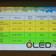
The color coordinates of the yellow hyperfluorescence revealed by Junji Adachi are (0.49, 0.50), the FWHM (Full Width at Half Maximum) is 76 nm, the EQE is 15.7% on 1000 nit basis, and the LT50 is 62,000 hours by 1000 nit. And the color coordinates of the green hyperfluorescence are (0.28, 0.65), the FWHM (Full Width at Half Maximum) is 31 nm, the EQE is 20.6% on 1000 nit basis, and the LT50 of 1,000 nit is 48,000 hours.

Junji Adachi also revealed the performance of Blue hyperfluorescence, which is currently under development. The maximum emission wavelength of the blue hyperfluorescence is 470 nm, the EQE at 1000 nit is 22%, and the LT50 at 750 nit is 100 hours. In particular, he predicted that the performance of Blue hyperfluorescence would be further improved in the future, saying that it began to improve rapidly in the first half of 2018.

In the following announcement, Dr. Georgios Liaptsis of CYNORA explained about the deep Blue under development, emphasizing that the wavelength should be 460 nm and the CIEy should be within 0.15. He revealed its performance, adding that CYNORA has been carrying out the necessary research to make the lifetime of deep Blue as long as that of sky Blue even with phenomenon that the life span is getting longer as the Blue goes closer to the sky Blue

Fluorescent blue is currently used for the Blue of all OLED applications. Attention is growing whether Blue TADF or Blue Fluorescence can be commercialized to realize better efficiency and lifetime than existing fluorescent blue.

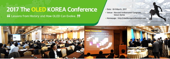
All about OLED in one place, UBI Research, ‘3rd OLED KOREA Conference’ will be held

UBI Research plans to hold the 3rd OLED KOREA Conference with the theme of “Lessons from History and How OLED Can Evolve” at Novotel Ambassador Hotel on Mar. 8 (Wed) to 9 (Thu).

The OLED industry is expected to grow rapidly according to the adaption of full-driven OLED panels by Sony and Apple in 2017 and the competition among panels, equipment, and manufacturing companies can be intensified at the same time. It is necessary to understand and respond strategically to industry trends for successful business under such circumstances. The opportunities to share ideas and concerns each other and close exchanges between Industry-academic institute, panel, materials and equipment companies have been required. UBI Research has prepared a place to freely exchange various information and opinions through the 3rd OLED Korea Conference by reflecting such needs of the industry.

The Korea Conference will be an opportunity to analyze the past trends of OLED which the usage and application range is getting wider and to discuss the successful advancement and strategies to grow the OLED industry for the future. Therefore, it will be a valuable time to practically help the OLED industry.

The Presentation is planned by twenty-four (24) domestic/international experts related to OLED display such as set and panel makers, materials/equipment companies, university/research etc. including UBI Research, Samsung Display, Cynora and CEREBA about followings:

▲Exploring new opportunities with OLED and the preparation, ▲Possible directions and the reasoning for OLED, ▲Lessons from the history and how OLED can be evolved, ▲OLED and its collaboration, investigating the possibilities

We will establish the opportunity to contribute to the growth of the OLED industry based on the sharing of mutual opinions by preparing a networking space between the companies through luncheon during the conference period and breakfast with OLED reception.

Detail information can be found in www.oledkoreaconference.com

CYNORA Achieves a New Milestone in Efficiency and Stability of Blue TADF Emitters for OLEDs

CYNORA, a leader in TADF (thermally activated delayed fluorescence) materials, has developed new material classes that combine both, high efficiency and long lifetime, for blue emission. With these new achievements, the company is on track to reach the performance requested by the OLED industry. The commercialization of CYNORA´s TADF materials is therefore still planned for the end of 2017.

Earlier this year, in May 2016, CYNORA had established two blue emitter systems where one of them showed a high efficiency while the other showed a long lifetime. During the last 6 months CYNORA has made further, significant progress by combining high efficiency and long lifetime in a single blue emitter system. In an OLED device, the new blue material reaches 14% EQE (external quantum efficiency) together with a lifetime of 420h (LT80, at 500 cd/m2, λ < 480 nm). With this performance, CYNORA has now shown that blue TADF emitters can reach OLED display specifications soon.

“Our constant progress on blue TADF emitters was made possible by our growing team of TADF experts and by the close collaboration with CYNORA’s customers” says Thomas Baumann, CSO at CYNORA, “We have developed several classes of high performance TADF materials which we are currently optimizing for market readiness at the end of next year.”

CYNORA’s dopants are fully organic and designed for existing vacuum deposition. The company will adapt the blue TADF emitters for solution processing in a second step. With its blue TADF technology CYNORA will enable device makers to provide OLED displays with significantly increased energy efficiency and higher display resolution.

UDC & Tianma Enter into Long-Term OLED Patent License and Supplemental Material Purchase Agreements

Source = UDC

Source = UDC

Hyunjoo Kang / jjoo@olednet.com

Universal Display Corporation( UDC ), enabling energy-efficient displays and lighting with its  UniversalPHOLED technology and materials, today announced the signing of an OLED Technology License Agreement and Supplemental Material Purchase Agreement with Tianma Micro-electronics Co. Ltd., a leading Chinese small-and medium-size display panel manufacturer. The agreements run for five years.

Tianma is a leading player in AM-OLED technology and series production capacity in domestic China . In late May, Tianma demonstrated its latest OLED advances with a number of display prototypes at Display Week 2016 International Symposium, Seminar and Exhibition. Tianma has a Gen 5.5 AM -OLED line in Shanghai , which started producing AM-OLED modules for intelligent mobile terminals to brand clients this year. Tianma is also increasing its OLED investments to ramp up capacity for commercial mass production.

“We are very pleased to enter into these license and supply agreements with Tianma Micro-electronics, an early OLED developer and key Chinese display maker,” said Steven V. Abramson , President and Chief Executive Officer of Universal Display . “Tianma has been at the forefront of OLED R&D in China for a number of years, and we look forward to working with Tianma to advance their commercial OLED product pipeline with our proprietary OLED technologies and materials. Around the world, we believe that OLED research, development and investment activities are gaining tremendous ground, as consumer demand for cutting-edge, fast-response, thin, energy-efficient displays continues to rise, in products such as smartphones, wearables, tablets and automotive.”

Under the license agreement, Universal Display , through its wholly-owned subsidiary UDC Ireland Limited , has granted Tianma Micro-electronics non-exclusive license rights under various patents owned or controlled by Universal Display to manufacture and sell OLED display products. Additionally, Universal Display will supply phosphorescent OLED materials to Tianma Micro-electronics for use in its licensed products.

UDC Announces Q2 2016 Financial Results

Source = UDC

Source = UDC

Hyunjoo Kang / jjoo@olednet.com

Universal Display Corporation( UDC ), enabling energy-efficient displays and lighting with its Universal PHOLED technology and materials, today reported financial results for the second quarter ended June 30, 2016.

For the second quarter of 2016, the Company reported net income of $21.8 million, or $0.46 per diluted share, on revenues of $64.4 million. This includes $1.8 million of currency exchange loss related to the BASF OLED patent acquisition. For the second quarter of 2015, the Company reported a net loss of $11.8 million, or $0.25 per diluted share, on revenues of $58.1 million. The 2015 net loss reflected a $33.0 million write-down of inventory, primarily of an existing host material and associated work-in-process. Excluding this item and its associated $1.9 million reduction of income tax expense, adjusted net income for the second quarter of 2015 was $19.4 million, or $0.41 per diluted share (see “reconciliation of non-GAAP Measures” below for further discussion of the non-GAAP measures included in this release).

“Our second quarter 2016 revenues and net income increased year-over-year, and we maintained our strong margin profile. We are confident that the underlying growth fundamentals of our long-term outlook remain robust, but near-term, we expect our revenue growth will be delayed by about six months,” said Sidney D. Rosenblatt, Executive Vice President and Chief Financial Officer of Universal Display.

Rosenblatt continued, “We expect strong revenue growth in 2017. At that time, new OLED production from the multi-year capital expenditure cycle is slated to start contributing to our revenues. Ahead of this wave of high-volume capacity, we have been working to expand and broaden our team and core competencies to advance our strategic initiatives and increase our competitive edge. We expect these initiatives, along with new OLED capacity, coupled with our pipeline of new materials, new technologies and new agreements, to bolster our long-term growth plan.”

Financial Highlights for the Second Quarter of 2016

The Company reported revenues of $64.4 million, compared to revenues of $58.1 million for the same quarter of 2015, an increase of 10.8%. Material sales were $22.3 million, down 8.3% compared to the second quarter of 2015, primarily due to a $2.0 million decline in host material sales. Royalty and license fees were $42.0 million, up from $33.7 million in the second quarter of 2015. The Company recognized $37.5 million in Samsung Display Co., Ltd. (SDC) licensing revenue in the second quarter of 2016, up from $30.0 million in the same quarter of 2015.

The Company reported operating income of $34.0 million in the second quarter of 2016, compared to an operating loss of $4.8 million for the second quarter of 2015. Excluding the inventory write-down of $33.0 million, adjusted operating income was $28.2 million for the second quarter of 2015. Operating expenses were $30.4 million, compared to $62.9 million in the second quarter of 2015 and cost of materials was $5.7 million, compared to $39.1 million in the second quarter of 2015, both of which included the inventory write-down of $33.0 million in the second quarter of 2015.

The Company’s balance sheet remained strong, with cash and cash equivalents and investments of $332.0 million as of June 30, 2016. During the second quarter, the Company added $96.0 million in intangible assets in the form of intellectual property purchases and certain other assets from BASF, increasing the portfolio to more than 4,100 issued and pending patents worldwide. During the second quarter, the Company generated $36.2 million in operating cash flow.

Financial Highlights for the First Six Months of 2016

The Company reported revenues of $94.1 million, compared to revenues of $89.3 million for the first half of 2015, or an increase of 5.4%. Material sales were $46.6 million, down 8.8% compared to $51.1 million in the first half of 2015, primarily due to a $7.0 million decline in host sales. Royalty and license fees were $47.4 million, up from $38.1 million in the first half of 2015.

The Company reported operating income of $36.7 million in the first half of 2016, compared to an operating loss of $3.1 million for the first half of 2015. Excluding the inventory write-down of $33.0 million, adjusted operating income was $30.0 million for 2015. For the first half of 2016, we reported net income of $23.8 million, or $0.51 per diluted share, compared to a net loss of $10.5 million, or $0.23 per diluted share, for the same period of 2015. Excluding the inventory write-down and the associated $1.9 million reduction of income tax expense, adjusted net income was $20.7 million, or $0.45 per diluted share, for the first half of 2015.

Operating cash flow for the first half of 2016 was $36.2 million, a decrease of 51.8% compared to $75.2 million for the first half of 2015 which included an upfront $42.0 million license and royalty payment.

2016 Guidance

While the OLED industry is still at a stage where many variables can have a material impact on its growth, based upon the most recent and best information on hand, the Company believes it is prudent to revise its 2016 revenues guidance. The Company now expects 2016 revenues to be in the range of $190 million to $200 million.
Dr. Andreas Haldi joins CYNORA as Chief Marketing Officer

Source = Cynora

Source = Cynora

Hyunjoo Kang / jjoo@olednet.com

CYNORA, a leader in blue TADF (thermally activated delayed fluorescence) materials, has appointed Dr. Andreas Haldi as its Chief Marketing Officer.

With his strong technical and business experience, Andreas Haldi will reinforce CYNORA in the forthcoming commercialization of its high performance blue OLED materials.

CYNORA is preparing the commercialization of its emitting materials for OLEDs. The company is hiring Andreas Haldi to further enhance its already good relationships with the major display makers and to now prepare with them the implementation of its materials in their products.

Andreas Haldi has close to 15 years of experience in the OLED materials field and profound knowledge of the Asian display market. Prior to joining CYNORA, Haldi held manager positions in R&D and sales at Novaled GmbH. For the last five years he was headquartered in Seoul, Korea, as Novaled’s representative in front of the major AMOLED display makers in Asia.

“I am very happy to get Andreas on board” says Gildas Sorin, CYNORA’s CEO. “We are preparing ourselves intensively for the commercialization of our blue emitters. Thanks to his proven skills on OLED and his experience in Asia, Andreas will help us to build up our success as a leading supplier for TADF materials.”

“I am looking forward to joining CYNORA” says Andreas Haldi, “CYNORA has shown its expertise and its impressive capability to progress rapidly during the last 8 months. CYNORA has a great potential to become key player in the OLED material industry.”

The appointment of the new CMO is a significant signal of CYNORA’s further development and its forthcoming market entry. Blue TADF-based emitters will enable a significant reduction of power consumption in OLED devices and will allow higher display resolution. CYNORA owns a broad IP portfolio with over 100 patent families and is aiming for over 600 patents.
UDC Announces Strategic Acquisition of Adesis

Source : UDC

Source : UDC

Hyunjoo Kang / jjoo@olednet.com

UDC announced today that it has entered into an agreement to acquire Adesis, Inc. Adesis is a privately held contract research organization (CRO) with 43 employees specializing in organic and organometallic synthetic research, development, and commercialization. Adesis is a critical technology vendor to companies in the pharmaceutical, fine chemical, biomaterials, and catalyst industries, and has worked with Universal Display over the last few years to help advance and accelerate a number of Universal Display’s product offerings.
“This acquisition is part of our strategic growth plan. We believe that it will provide additional highly-skilled resources to further advance our initiatives for the development and delivery of next-generation proprietary emissive material systems in the rapidly evolving OLED industry,” said Steven V. Abramson, President and Chief Executive Officer of Universal Display. “Moreover, we expect it to enable us to leverage our twenty-plus years of experience in developing and commercializing cutting-edge chemistry technologies to help expand Adesis’ businesses across its end-markets including pharma, biotech and catalysis. We are delighted to welcome Dr. Andrew Cottone, President of Adesis, Dr. Ving Lee, Chief Scientific Officer, and the vastly experienced Adesis team to UDC.”
“We are very excited to become part of UDC and build additional synergies between both companies, and further enhance the growth of UDC’s OLED leadership,” said Andrew Cottone, President of Adesis, Inc. “In addition, we anticipate that Adesis will benefit from UDC’s financial and business acumen to better support our clients with world-class technology and expertise, and reinforce our positioning for continued growth as a specialty chemical CRO.”

Under the terms of the agreement, Universal Display will acquire all outstanding shares of Adesis, Inc. in a merger for approximately $36 million in cash. The transaction is expected to close in the third quarter of 2016, subject to customary closing conditions. Following the closing, Adesis will operate as a wholly-owned subsidiary of Universal Display Corporation. Andrew Cottone will continue as the President of Adesis, and Steve Abramson will become the Chairman of the Board of Adesis.

OLED Tail Light for First Time in Volume Produced Audi Cars

Source = Novaled

Audi car. (Source = Novaled)

Hyunjoo Kang / jjoo@olednet.com

R2D2, a joint project to analyze and to develop high-TRL processes and technologies for manufacturing of flexible OLED funded by the German Federal Ministry of Education and Research (BMBF) has been successfully completed. The goal was to work on OLED technology for reasonable priced OLEDs which could easily be employed to manufacture marketable products.

Meanwhile, AUDI AG is offering glass-based OLEDs in a high-volume production model for the first time as the tail lights for the TT RS. The transition to a production-ready OLED product has been achieved through the advances from the R2D2 project. “The R2D2 Project funded by BMBF has brought OLED technology in Germany a good deal further. Sectors beyond lighting and Automotive will follow suit. There are already prospective designs for household appliances and even for aircraft over the long term,” says Project Coordinator Dr May of Fraunhofer FEP. Besides FEP, also AUDI AG, Diehl Aerospace GmbH, HELLA KGaA Hueck & Co., OSRAM OLED GmbH, VON ARDENNE GmbH and Novaled were consortium partners.

Novaled was able to optimize the OLED layers and to develop and provide a set of materials to meet the challenging specifications of the automotive industry. Cost-effective solutions were devised. This included providing mass production stable materials for easy and efficient employment in mass production, as well as saving development time by generating methods that can ascertain the compatibility of new organic materials with manufacturing processes.

One of the success factors of R2D2 was that project partners could cover the whole value chain: from material research to equipment construction, component technology through application studies for future products.

The consortium would like to thank the German Federal Ministry of Education and Research (BMBF) for funding the project “R2D2” with a grant of 5.9 million Euros over a 30-month period.

UDC, net income $1.9 million for 1Q 2016…46% ↑ YoY

Source : UDC

Source : UDC

Hyunjoo Kang / jjoo@olednet.com

UDC (Universal Display Corporation), enabling energy-efficient displays and lighting with its UniversalPHOLED® technology and materials, today reported financial results for the first quarter ended March 31, 2016.

For the first quarter of 2016, UDC reported net income of $1.9 million, or $0.04 per diluted share, on revenues of $29.7 million, compared to net income of $1.3 million, or $0.03 per diluted share, on revenues of $31.2 million for the first quarter of 2015.

“In the first quarter, our commercial emitter revenues grew 8% year-over-year, primarily driven by strong green emitter shipments. Royalty and license fees increased by 22%. Host material sales, in line with expectations, declined year-overyear,” said Sidney D. Rosenblatt, Executive Vice President and Chief Financial Officer of UDC

Rosenblatt continued, “The OLED landscape continues to expand. New OLED products are launching, capacity is building, equipment bookings are increasing and the pipeline of OLED design activities is broadening.

With OLED display penetration at only about 10% of the total consumer electronic display market, new applications like automotive, virtual reality, augmented reality and signage emerging and OLED lighting transitioning from development stage to commercial, we believe that our long-term growth trajectory remains strong.”

Financial Highlights for the First Quarter of 2016 The Company reported revenues of $29.7 million, compared to revenues of $31.2 million in the same quarter of 2015.

Material sales were $24.3 million, down 9% compared to the first quarter of 2015, primarily due to a $5.0 million decrease in host material sales. This decline was partially offset by an increase of $2.5 million in emitter material sales.

Royalty and license fees were $5.3 million, up from $4.4 million in the first quarter of 2015.

No revenue was recognized under the Samsung Display Co., Ltd. (SDC) licensing agreement in the first quarter, as SDC is obligated to make licensing payments in the second and fourth quarters of the year. For 2016, the Company expects to recognize $75 million in SDC licensing revenues for the full year.

The Company reported operating income of $2.5 million, up from $1.8 million for the first quarter of 2015. Operating expenses were $27.2 million, compared to $29.5 million in the same quarter of 2015.

Cost of materials was $5.1 million, compared to $8.6 million in the first quarter of 2015, reflecting the decline in host material sales volume, which have less favorable margins than the Company’s emitter materials.

The Company’s balance sheet remained strong, with cash and cash equivalents and investments of $395.7 million as of March 31, 2016.

Adoption of Idemitsu’s Material in LG’s OLED TV

Source : Idemitsu Kosan

Hyunjoo Kang / Reporter / jjoo@olednet.com

Idemitsu Kosan Co.,Ltd.´s (Head Office: Chiyoda-ku, Tokyo; Representative Director and CEO: Takashi Tsukioka, hereinafter “Idemitsu”) OLED material will be used for LG Electronics Japan Inc.´s (Head Office: Chuo-ku, Tokyo; President: In-gyu Lee) latest OLED TV which will be released in Japan this coming mid-May. An

An OLED TV is a next-generation television that has a display which eliminates the need for backlight, which is different from an LCD TV.

Eliminating the need for backlight makes it possible to not only provide a curved and super-thin display but to also represent jet black without being affected by the illumination of the backlight.

Idemitsu has studied and developed OLED materials since the 1980s and has a particular advantage in the development of high-performance blue light-emitting materials. In addition, Idemitsu also has many related patents and manufacturing plants in both Japan and South Korea, and supplies materials to a variety of manufacturers.

After the agreement to form a strategic alliance regarding the OLED business in 2009, Idemitsu and the LG Group concluded an agreement for mutual cooperation in the field of OLED technology and device-related patent licensing in December 2014.

As leading companies, each company has achieved results in product development through their active efforts in this field.

As a result of concluding the agreement, Idemitsu´s OLED material will be used for LG Electronics´ latest television to be released in Japan following the world´s first large high-definition OLED TV which was released by LG Electronics in 2013.

Both companies will continue to provide technical cooperation to develop materials and products that will popularize the use of OLED displays.

OLED Emitting Material Market, To Grow into US$ 560 Million in 2015

According to ‘’OLED Emitting Material Annual Report’’ published by UBI Research on 13 March, OLED emitting material market of 2015 is forecast to grow into US$ 560 million, a 16% growth compared to 2014. The report analyzed that active operation of LG Display’s E4 (M2) line, and operation of Samsung Display’s A3 line, and an increase in operation rate by existing A1 and A2 lines are the main cause for the market growth. Additionally, due to the intense mass production start by the latecomers and expansion of large area OLED panel market, the OLED emitting material market is estimated to grow by 35% compound annual growth rate, and form approx. US$ 2,500 million market in 2020.

In terms of countries, Korea occupies the most of 2015 OLED emitting material market with its market share of 90% or higher. However, from 2017, with China’s bold mass production, China is expected to hold market share of over 20% or higher. Thus, emitting material companies are projected to target Chinese market.

AMOLED panel applied to Samsung Elec.’s Galaxy S6 and S6 Edge, which were revealed in MWC2015, utilized new supply chain and it is estimated these will be used for AMOLED panels of future products. Dow Chem.’s phosphorescent red host materials were chosen for the new supply chain.

<OLED Emitting Material Market Forecast Source: UBI Research><OLED Emitting Material Market Forecast Source: UBI Research>

Regarding this matter, the head of UBI Research Dr. Choong Hoon Yi will give an in-depth presentation titled ‘The Future of OLED’ discussing OLED emitting material market and OLED industry at the 1st OLED Korea Conference. The 1st OLED Korea Conference will be held in SC Convention in Gangnam, Seoul, South Korea on April 2.