How far has QNED completed?

The reality of QNED (quantum dot nano-rod LED), which Samsung Display is preparing as a next-generation display, has become clear.

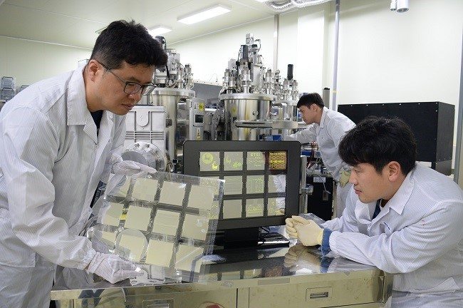
As a result of analyzing 160 patents applied by Samsung Display, it was confirmed that the structure constituting the QNED has already been completed, and that the only remaining task is to keep the number of nano-rod LEDs arranged in the light-emitting pixel constant.

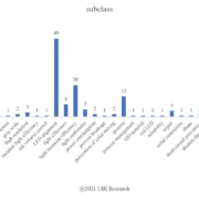
As a result of classifying the contents of each patent according to the purpose of the application, a total of 39 types were found, with 49 cases related to device arrangement being the most. The following is 20 cases to improve the light efficiency.


The number of aligned nano-rod LEDs per pixel, which determines the yield and image quality characteristics of QNED, is determined by the distribution of LEDs in the ink, the number of LEDs injected into the pixel, and the alignment ratio of the injected LEDs.

If the distribution of the number of nano-rod LEDs per pixel is different, there is a change in the voltage applied to each pixel, resulting in a defect.

It has been confirmed that Samsung Display has already developed a method for making the number of nano-rod LEDs per pixel constant and an algorithm that can make the luminance uniform even when the number of nano-rod LEDs is different.

In the “QNED Technology Completeness Analysis” published this time, it was written as the contents of the previous report published through analysis of 94 patents and 66 newly added patents. It was analyzed and recorded.

In this report, QNED patent numbers, classification tables, and quantitative analysis data that have not been disclosed before are provided in Excel.

OLED Market Enters Adjustment Period from Rapid Growth

As smartphone makers, including Samsung Electronics and Apple, increased the use of OLEDs in flagship models, the growth of the OLED market, which had been rapidly growing, has been braked.

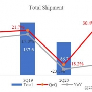
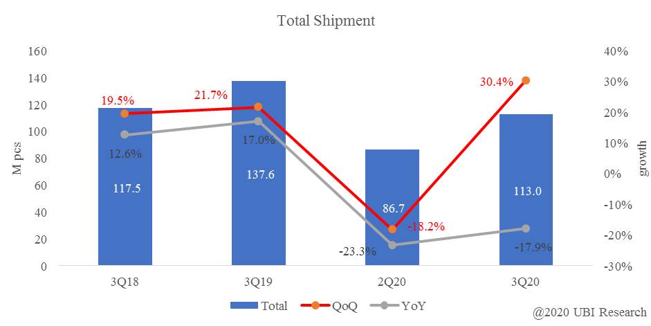
The third quarter of each year is the season with the best OLED performance for smartphones due to the launch of a new iPhone. According to the display market track of UBI Research (www.ubiresearch.com), in the third quarter of this year, 113 million units were shipped, an increase of 26.3 million units compared to 86.7 million units in the last quarter, showing a growth of 30.4%. However, this figure is due to an optical illusion. The reason is that the results in the first and second quarters were very poor compared to before due to COVID-19. Compared to the third quarter of last year, shipments in the third quarter of this year decreased by 17.9%. Shipments are smaller than in the third quarter of 2018.

The decrease in OLED shipments for smartphones in the third quarter is due to the addition of Huawei sanctions to COVID-19. The sharp drop in shipments from Samsung Display and BOE to Huawei deteriorated the third quarter earnings.

There are also many analyzes that companies such as Samsung Electronics, Oppo, and Vivo will benefit from the reflection due to Huawei sanctions. However, since Samsung Electronics is currently struggling in the Chinese market, and the brand power of Oppo and Vivo is less than that of Huawei, it will be difficult to replace the expensive smartphone market in China occupied by Huawei. Therefore, Huawei’s smartphones, which mainly use OLEDs, disappear from the market, and shipments of Samsung Display and BOE are also forced to decrease more than expected.

The growth of the smartphone OLED market is expected to slow for the time being due to Huawei’s smartphone production disruption, which was expected to break through the 300 million units’ market and purchase OLED in large quantities. As a result, the OLED market in China will suffer a severe oversupply situation.


Samsung Electronics’ foldable smartphone to be released in 2021, with touch pen and UTG thickness different?

According to the ‘2020 OLED Components and Materials Report’ recently published by UBI Research, Samsung Electronics’ next-generation foldable smartphones to be released in 2021 are expected to be equipped with a pen function.

It is expected that the pen function will be added to Samsung Electronics’ Galaxy Z Fold2, which was released in September, but the flexibility issue of the digitizer, which is an essential material to support the pen function, and ultra thin glass (UTG), the cover window material. The pen function was not added in the end due to its thin thickness.

In order to add a pen function, Samsung Display seems to be considering applying an active electrostatic solution (AES) method that does not require a digitizer and changing the thickness of UTG.

First, the’Galaxy Note’ series uses an electro-magnetic resonance (EMR) method with a digitizer at the bottom of the OLED panel. The EMR method has good touch sensitivity and does not require a battery to be embedded in the pen, but it is not applicable to foldable devices due to the flexibility issue of the metal digitizer.

Unless the companies developing the EMR method provide a special solution, the AES method is highly likely to be applied to the pen for the next ball double device. In this case, the sensor pitch of Y-OCTA is formed more densely or the Touch IC is more complex. Can be designed.

The AES method is also being developed by LG Display and BOE to apply to foldable devices.

In addition, the thickness of UTG is also expected to change. The 30 um thick UTG, which is currently commercially available, has good flexibility, but due to its film-like characteristics, when pressure is applied with a touch pen, traces remain and may affect touch sensitivity. To solve this problem, Samsung Display is developing UTG with a thickness of more than 60 um in cooperation with glass processing companies.

As the thickness of the UTG decreases as the thickness increases, it is expected that the UTG currently under development will be applied with a concept in which the folded part is processed thin and filled with a material having the same refractive index as glass. In addition, in the future, there is a possibility that an additional coating process will be added after the reinforcement process without a protective film such as PET on UTG.

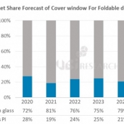
In UBI Research’s ‘2020 OLED Parts and Materials Report’, Samsung Display’s expected change in foldable OLED was written as a roadmap and the trends of related materials were analyzed. According to the report, Samsung Electronics’ application of pens for foldable devices is expected in 2021, and UTG materials are expected to lead the market at 78% by 2025 in the future cover window market for foldable devices.


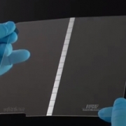
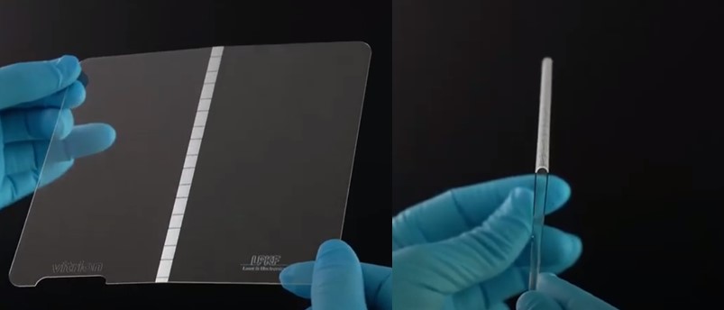
LPKF’s laser glass processing technology, makes a cover glass thicker than UTG be folded.

It was expected that the S Pen would be applied to Samsung’s ‘Galaxy Z Fold2’, which will be released in the second half of this year, but it has passed the year.

UTG, the cover window material currently applied to Samsung Electronics’ ‘Galaxy Z Filp’, is 30 um thick and is 1/10 thinner than 300 um, the thickness of commercially available cover glass.

It was possible to have flexibility by using UTG into a foldable phone, but due to the film-like characteristics, there was an issue that durability was insufficient to apply the S Pen.

In order to handle this issue, a technology that increases the thickness of UTG and secures flexibility will be needed. A typical method is processing the folding part of the glass to get flexibility even at a thick thickness.

LIDE (Laser induced deep etching) technology, developed and patented by German high-tech company LPKF, is expected to be a good example. It is known that this technology is a two-step process called micro-region transformation and chemical treatment using a laser, and can process glass of various thicknesses from 30 um to 900 um without micro crack.

LPKF explains that the part where the cover glass is folded is finely processed with a laser to give flexibility to the glass, and it is possible to design the pattern to be invisible using a polymer having same reflectivity as a cover glass.

If you look at Vitrion’s YouTube video (https://youtu.be/Vh3rU4LRHaw), a separate brand related to LIDE, in LPKF, you can see that a cover glass with a thickness of 500 um was patterned to secure bending radius of 1 mm.

<LPKF foldable OLED cover glass, Source: LPKF>

With this glass processing technology, attention is paid to whether a S-pen can be supported as a thicker cover glass is applied to a foldable phone in the future.

Samsung Display A3 line replaced with Y-OCTA manufacturing line

The touch panel technology installed on a mobile phone is an important element technology that performs a user interface function. Touch technology is changed from an add-on type to an on-cell type in flexible OLED displays.

The built-in method in which a touch sensor is formed on a thin film encapsulation (TFE) is called by various names such as Y-OCTA(YOUM on-cell touch AMOLED), ToE(touch on encapsulation) or FMLOC(flexible multi-layer on cell touch) for each panel maker. Unlike the add-on type, the on-cell type touch sensor is formed directly on the top of the encapsulation layer without a separate base film. Due to this, the on-cell type has a higher process difficulty than the add-on type, but it is advantageous to manufacture a thin OLED panel thickness, and there is an effect of reducing the process cost.

Recently, in order to apply this on-cell type touch technology to mobile phones using OLEDs, each display manufacturer is undergoing a step-by-step line modification work. Four mask steps are added to apply the on-cell type touch technology. There are two ways to cope with this process step increase: to install and respond to new equipment as much as the process to increase, and to proceed with the process at existing facilities.

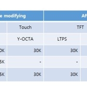
Samsung Display decided to use an existing exposure machine to use the on-cell type touch technology in the existing A3 line (Tangjeong), and is in the process of remodeling the 105K capacity TFT production line. In the existing process flow, a back plane process is performed with mother glass of 1500×1800 mm2 and 1500×900 mm2 glass with half-cutting of this mother glass is processed in the OLED process. Therefore, in order to process the half-cut glass again in the back plane equipment, the jig manufacturing method of connecting and processing two cut sheets is applied. After this modification, the production capacity of the A3 line will be reduced. The amount of 105K of the A3 line that is currently being renovated is changed from LTPS process to LTPO process, and it is combined with Y-OCTA process. In this case, 3 mask steps increase as LTPS is changed to LTPO, and 4 additional mask steps increase for Y-OCTA. As a result of the total increase of 7 mask steps, the A3 line is expected to reduce the existing 105K production capacity to approximately 75K level after remodeling.

China’s BOE is also constructing built-in touch processes in B7 and B11. BOE is in the process of adding and processing exposure equipment, etc. as a way to add a built-in touch process. In this case, there will be no significant change in production capa.

<Production capacity comparing with before/after modifying at SDC A3 line>

QNED structure and manufacturing technology analysis report published

UBI Research (www.ubiresearch.com) published “QNED Structure and Manufacturing Technology Analysis Report”, which analyzed 41 cases of Samsung Display’s QNED (quantum dot nanorod LED) published patents.

The contents described in this report were selected from the 41 patents published, which are considered to be used for QNED manufacturing, and are constructed by qualitative analysis.

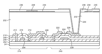
As a result of analyzing the published patent, the QNED structure was formed of TFT, pixel, and QD (quantum dot) -CF (color filter). In the published patent, all TFT structures are depicted as 2Tr (transistor), but it is estimated that a 3Tr1C structure will be used because at least three TFTs for current driving are required. The pixels consisted of nanorod LEDs, electrodes, and optical structures to increase light efficiency.

Until now, the electrode structure of the pixel was known to be rectangular, but as a result of analyzing published patents, the electrode structure is estimated to be circular. In a specific patent, when the asymmetric waveform was applied to the circular electrode, the alignment direction and alignment characteristics of the nanorod LED were improved. It is judged that the nanorod LED alignment electrode and the drive use the same electrode.

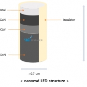
The nanorod LED used for QNED manufacturing is made of GaN and emits blue light, and the size is <1um x 10um. In order to increase the alignment effect of the nanorod LEDs and reduce process defects, the nanorod LED surface appears to be treated with an insulating film and an orientation radical.

The next full-screen display trend is the under-display camera

Reporter : Daejeong Yoon

Since Samsung’s Galaxy S8 and Apple’s iPhone X launch, smartphones with the Home button removed have become a trend in the smartphone market.

Due to the nature of smartphones that cannot grow indefinitely, display sizes with a large proportion within limited smartphone sizes are directly related to the competitiveness of smartphone set makers.

Samsung’s Galaxy S10, which was recently released, attracted great attention with its flexible OLED with HIAA (hole in active area) technology. Notch or HIAA designs, however, can still interfere with video viewing and gaming because camera lenses occupy a small portion of the display.

That is why a number of panel makers are developing under display camera technology for a full-screen display.

Under display camera technology allows the front camera to be placed behind the display for a full-screen display. Oppo unveiled the first smartphone with the technology at MWC China 2019, and BOE and Visionox also anticipated that under-display cameras will become the next trend in smartphones at CIOC 2019.

It is expected that screen, camera module, and algorithmic technologies will all be specially designed to implement under display camera technology. Specifically, the technology to make the pixel near the camera at low resolution to secure transmittance, to mount a CMOS image sensor of a larger pixel size than the existing, and to apply algorithm technology to improve the picture quality.

The trend of full-screen smartphones, which began in 2017, is paying attention to whether full-screen smartphones will bloom with the technology of under-display cameras since 2020.

[28TH FINETECH JAPAN] Sharp, announced Future Strategy Combining IGZO and OLED

Mr. Atsushi Ban, Vice President of Sharp presented a future strategy that combines IGZO and OLED through a keynote session at the 28th FINETECH JAPAN, held in Makuhari Messe, Japan from December 5, 2018.

Ban emphasized “The proportion of OLED in the entire display market is expected to grow even higher, and the new value of OLED is no different than flexibility.”

He said, “Sharp is also planning a variety of applications using the thin, light-weight and flexible characteristics of OLED. From the third quarter of 2018, its Taki plant has produced 4.5G backplanes and the Sakai plant is under injecting glass for OLED and module processing for 4.5G 15K quantity.”


Ban also pointed out the possibility of expanding the OLED industry through flexible OLED, commenting that Sharp’s next goal is to develop foldable OLED that combines IGZO. Sharp has pioneered a new display technology, called IGZO, which has been known for its semiconductor properties for years, but Sharp has developed a crystalline form that maximizes its benefits for greater display performance, and IGZO improves the performance of display panels in three significant ways: lower power consumption, higher resolution and special benefits for touch-sensitive displays. Ban expected that it could create new value if IGZO is combined with medium to large sized foldable OLED or rollable OLED.


Finally, Ban introduced Sharp’s IGZO development roadmap and announced that it will develop much improved IGZO.

Apple adopts LTPO TFT to extend battery life time to Apple Watch Series 4

Reporter & Analyst : Daejeong Yoon

Apple released its Apple Watch Series 4 with enhanced healthcare features on a larger screen than before, in the Steve Jobs Theater at Apple Park in California, USA on September 12.

<Apple Watch Series 4, Source: Apple.com>

In this announcement, Apple brought Apple watch series 4 with a new technology called LTPO to improve power efficiency.

LTPO stands for low temperature polycrystalline oxide. It is a kind of TFT using only the advantages of poly-Si with good charge mobility and IGZO with low power driving. LTPO TFTs have low leakage current and good on / off characteristics, which lowers power consumption and increases battery life.

<Apple’s LTPO TFT patent>

In addition, Apple increased the size of its Apple Watch 4 to 40mm and 44mm. The edge-to-edge screen is 35% and 32% larger than previous models by narrowing the bezel compared to previous models. The screen resolution was 368×448 pixels for the 44mm model and 324×394 pixels for the 40mm model. The display of Apple Watch4 is a plastic OLED made by LG Display with a maximum brightness of 1,000 nit. The Apple Watch Series 4 starts at US$399 for GPS model, while the cellular model starts at US$499. The Apple Watch Series 4 is available for pre-order from Septmber14 in the U.S. with the availability beginning September 21.

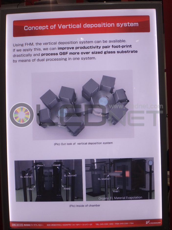
OLEDON, is to announce belt-plane source deposition technology for manufacturing ultra-high resolution and ultra-area OLED

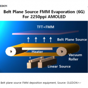
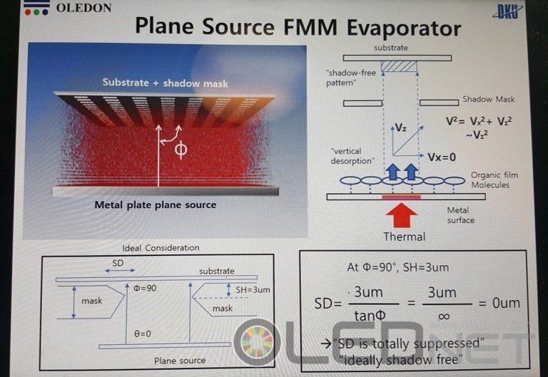
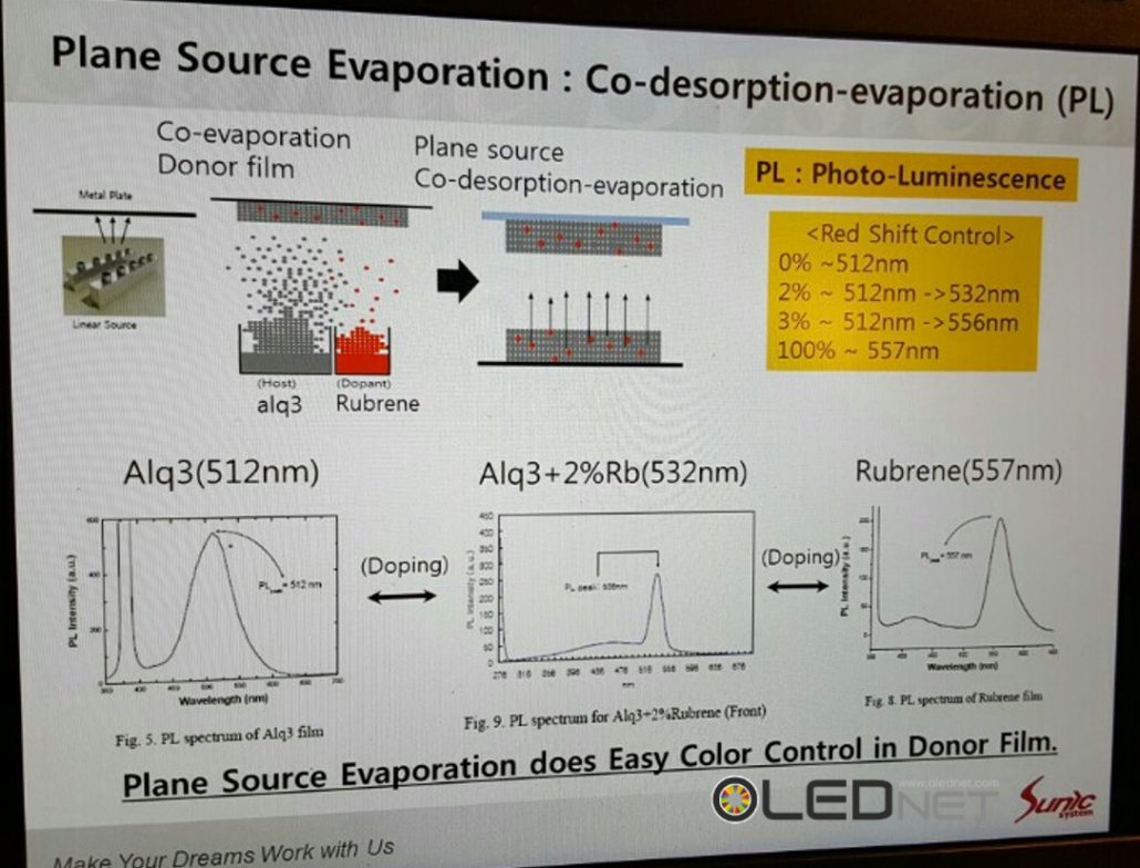
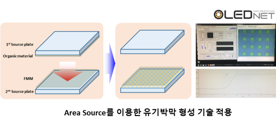
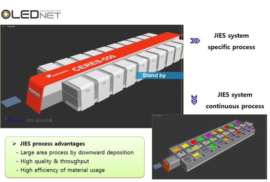
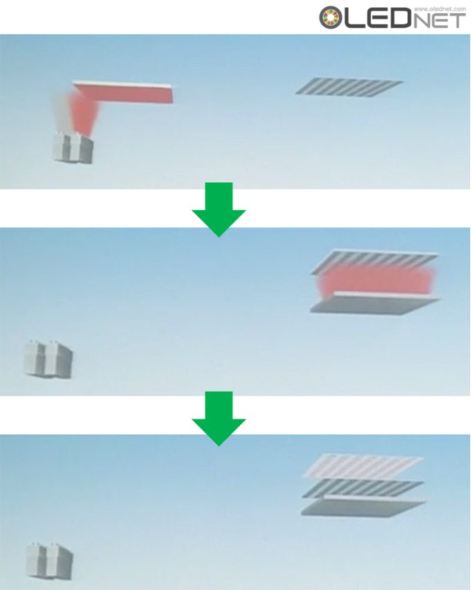
Plane source technology, which was first developed by OLEDON in the world, has the principle of depositing the first organic material on the metal surface and evaporating it upwards to produce fine pattern of 2250 ppi, which is ultrahigh resolution. In this plane source process, three processes such as the first deposition, the plane source inversion, and the second evaporation are necessary, and the number of the high vacuum chambers is increased when the mass production is applied. The belt plane source FMM deposition technology introduced by OLEDON has a concept of carrying out the above processes at a time in one evaporation equipment. This is a continuous plane source supplying deposition technology in which the metal surface is formed in a belt shape.


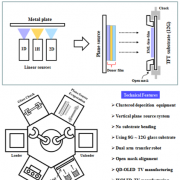
Hwang added, “Using vertical plane source enables smooth deposition process for the 12th generation class area substrate for QD-OLED TV without sagging problem. Vertical belt-plane source evaporation equipment adopts the concept of depositing the substrate in a standing-up position so that the load on the framed glass chuck and the open mask is very low. Thus, easy transportation of the substrate, and uniform deposition process of thin film over a very large area in the static state are possible.” This technology is expected to be applicable not only to the 8th generation but also to the cluster type mass-production evaporator with substrate sizes more than 10 generations in the future.


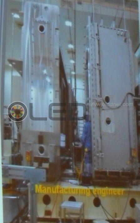
<Vertical belt plane source evaporator for QD-OLED, Source: OLEDON>

Commenting finally that the company has successfully completed the material denaturation test for blue materials and the blue dopant deposition test, Hwang expected the plane source deposition technology to be applied to both small & medium sized OLED and large area OLED manufacturing in future.

On the other hand, OLEDON holds more than 30 related patents including original patents of plane source and belt plane source evaporator. Also, the company recently filed a patent related to a vertical belt plane source evaporator for mass production.


OLEDON unveils plane source deposition technology for ‘super-gap’ OLED manufacturing.

Attention is growing since OLEDON, a venture company developing OLED deposition equipment, unveiled plane source deposition technology for OLED manufacturing to maintain ‘a superb gap with the competing countries’, at IMID2018, held in COEX, Seoul, Oct. 24, 2018.

Hwang Chang-Hoon, CEO of OLEDON, said, “Korea should actively invest in the development of creative deposition technology to maintain the first place in the current OLED producing countries.” He expects that plane source deposition technology is to be used both for small and medium size OLED and large area OLED manufacturing in future.
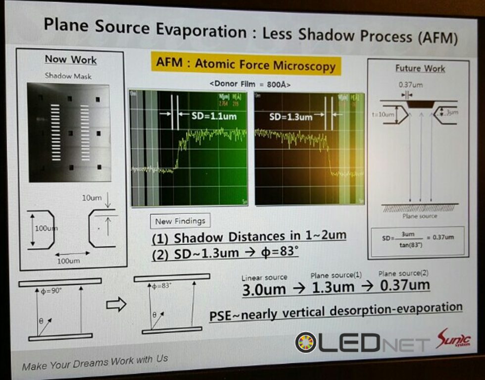
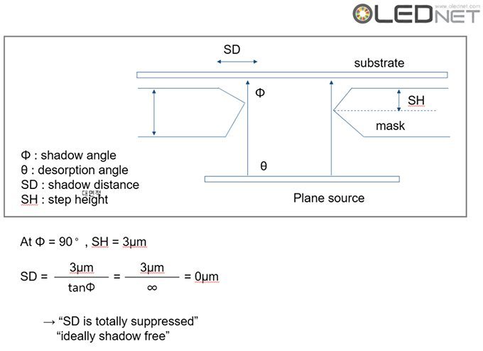
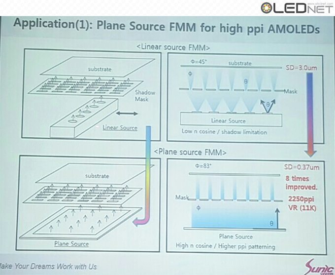
OLEDON is developing the world’s first curved plane source FMM deposition technology, which is an ultra-high-resolution OLED deposition technology capable of manufacturing 2250ppi AMOLED. The shadow distance of fine pattern can be up to 0.18um, enabling 11K high-resolution AMOLED pattern process.


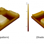
<Existing FMM deposition pattern (left) and plane source FMM deposition pattern (right), Source: OLEDON>

According to Hwang, this process was confirmed with 800 ppi shadow mask, and the emission area of the pattern deposited with plane source was 1.7 times higher than the conventional deposition method.
On the other hand, OLEDON holds the original patent for the FMM deposition technology of plane source, and has recently applied for a patent for vertical plane source deposition for large area OLED TV manufacturing.


<Vertical plane source deposition for OLED TV manufacturing, Source: OLEDON>

OLEDON develops vertical plane source deposition technology for large OLED TV manufacturing

Hwang Chang-Hoon, CEO of OLEDON, which has developed plane-source deposition technology for small & medium-sized OLED and large area OLED, said that it is under development of vertical plane source deposition technology capable of manufacturing ultra-large OLED TVs of 77 inches or larger. Hwang introduced the related technology that it is possible to mass produce OLED TVs of 77 inches or more without the sagging problem of large substrate such as 12th generation (3300 x 4000 mm) substrate when using vertical plane source deposition technology.

According to Hwang, the production yield for 75 inch TVs or larger with the conventional inline type evaporator might be very low due to severe sagging of the substrate and difficult control of many linear sources. To solve this problem, Hwang said that a new 12-generation large-area cluster-type deposition technology is needed, and that vertical plane source deposition technology will be an appropriate alternative.

On the other hand, OLEDON holds the original patents for plane source deposition technology. It also filed a patent related to the curved plane source FMM deposition for high-resolution AMOLED manufacturing, and a patent related to the vertical plane source deposition technology for manufacturing large-area OLED TV.

LG Display “Strategic direction is OLED. Uncompetitive LCD lines are planned to be switched.”

In the 2Q earnings release conference call hosted on the 25th July, Kim Sang-don, LG Display CFO, said, “Looking back at the first half of 2018, the market was in a difficult situation due to the slump in prices, the traditional off-peak season and increased display supply from China. We expected the market conditions to be stabilized in the first half of this year from the bad market condition of the second half of last year, but it has continued to decline more rapidly and steeply. However, with starting the second half of 2018, it has been observing that the price is rising since July owing to upcoming favorable seasonality and customer restocking.”

“Although the market situation has changed favorably in the second half of the year, it is different from the past supply and demand cycle because of the uncertainty of forecasts. Moreover, the oversupply and asymmetric competition in the display market are unavoidable.” LG Display announced that it will maintain its conservative strategy in the second half of the year as the unpredictability is still high.

LG Display’s sales revenue in the second quarter of 2018 was KRW 5,611 billion, decreased by 15% compared to the second quarter of 2017. Operating loss in the second quarter of 2018 recorded KRW 228 billion. This compares with the operating loss of KRW 98 billion in the first quarter of 2018 and the operating profit of KRW 804 billion in the second quarter of 2017. The company suffered a large deficit due to a continued and steep decline in panel prices and lower demand in panels following the previous quarter. Although the shipment was increased by 2% QoQ, the selling price per area (m2) was decreased by 4%.

As a positive indicator, the TV panel price fell sharply, but the overall panel price decline was only 1% due to the competitive position of OLED panels. The market is anticipated to turn into positive situation in the third quarter, compared to the first half of the year, since panel shipments are expected to increase with the orders to restock the inventory.

LG Display, which is currently conducting both LCD and OLED business with small and medium sized panels and large area panels, mentioned clearly about its future strategic direction including the direction for the second half of the year as “concentrating on OLED business and focusing on high value of LCD business” in this conference call.

LG Display announced that it will focus more on differentiated LCD features and technologies in the IT sector such as narrow bezel, IPS borderless, and oxide technology, as well as high-value-added products such as larger-size TV panels and commercial displays, considering that a structural oversupply in panels and fierce competition among display makers are expected to continue down the road.

In addition, LG Display will achieve a turnaround to profit in the OLED TV sector in the third quarter of 2018. By making its final decision to invest in its Gen 10.5 OLED panel production line in Paju, Korea, and by starting mass production in the latter half of 2019 at its Gen 8.5 OLED production line now under construction in Guangzhou, China, LG Display will accelerate the expansion of the global large-size OLED market. Furthermore, additional production facilities for OLED 8.5 generation are known to be considered with the plan that the rationalization of LCDs during the year is also to be implemented although there was no direct mention of the timing and specific lines. For the plastic small and medium-sized OLED panel business, which is experiencing difficult times, compared to large area OLED, for which LG is expanding the production capacity in response to increasing demand, it said that they are preparing for future markets with the necessary strategic technologies with the emphasis of mobile and automotive markets. The E6-1 line, which has been mentioned as a production plant for Apple, is expected to begin mass production in the fourth quarter of this year, revealing the possibility of a possible supply of display to the iPhone OLED model in 2018. In addition, demand for OLED panels is increasing in the automobile market, and it is expected that full-scale business will start in the second half of next year. At the current order backlog, it is confirmed that OLED panels are in the late stage of about 10%. This means that much of the work has already been done. Finally, LG Display is well aware of the lack of funding and funding shortfalls over its competitors in relation to its future preparations. The company plans to reduce its capex by about 3trillion won by 2020, with a substantial portion of depreciation and amortization It is possible through internal working capital management and it plans to borrow the rest. LG Display confirmed that it has not reviewed the rights issue several times in the market, and LG Display has thoroughly prepared a variety of OLED portfolios, revealing its commitment to success by differentiating it from its competitors in the area of latecomers.

LCD Smartphone is 4K era, what about OLED Smartphone?

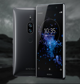
In the past MWC 2017, Sony unveiled the world’s first Smartphone with 4K LCD and it is scheduled to release the Xperia XZ2 Premium with 4K LCD on July 4. Attention is growing whether 4K resolution market is to be launched in earnest in smartphones.

<Xperia XZ2 Premium of Sony, Source: theverge.com>

TV market is already moving beyond the 4K to the 8K. Samsung Electronics and Sharp released new TVs with 8K resolution in the first half and Sony plans to release 8K TVs in the second half. LG Display also exhibited 88inch 8K OLED TV at CES 2018. As such, 8K TV is entering the premium TV market, and smart phones are expected to increase the number of products with 4K resolution in response to the higher resolution of TVs.

In the Smartphone, 4K has been implemented in LCD; however, in the case of OLED, QHD resolution is still dominant for the 4 consecutive years.

<Resolution change of Samsung Galaxy series, Source: UBI Research DB>

This is because there are many restrictions on the fine metal mask (FMM) technology that is being applied to OLED manufacturing. The thickness of FMM applied to the current production is about 20 ~ 30um. For 4K fabrication, the thickness should be as thin as 10um, but it is difficult for existing FMM manufacturing method.

As a result, FMM replacement technologies are being developed for high resolution implementation. Typical technologies under developing, include laser FMM patterning with laser, electroforming manufactured by electroplating method, a fine hybrid mask that is used to form a frame by electroplating on a film and pattern the film with a laser, and a surface source that realizes a high resolution by vertically setting the deposition incident angle.

Deposition technologies for high-resolution manufacturing at various exhibitions and conferences are being introduced. Depending on the availability for securing mass production, it is expected to see not only 4K OLED Smartphone, but also high-resolution AR and VR devices of RGB method.

Sony, announced the commercialization of 0.5-inch micro OLED with UXGA resolution

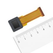
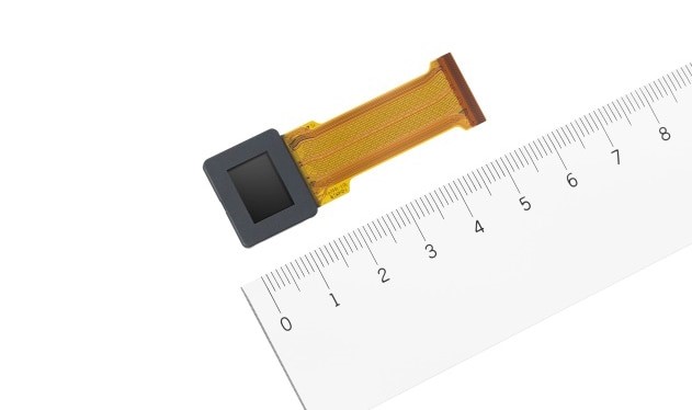
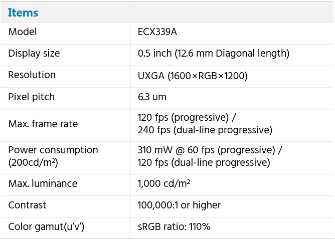
Sony announced the upcoming release of the ‘ECX339A’, a 0.5-inch OLED micro-display with UXGA resolution. According to Sony, it has achieved the world’s smallest pixel pitch of 6.3 μm, enabling a resolution 1.6 times higher than its predecessor, “ECX337A “(0.5-inch QVGA (1280 × 960)).

<Sony’s 0.5 inch micro OLED ‘ECX339A’, Source: sony.co.jp>

By employing newly-designed peripheral circuits that operate on half the voltage of previous model, it supports a high frame rate of up to 240 fps, with dual line progressive driving technique and low power operation.

<Comparison of OLED resolution between new product(left) and previous product(right), Source: sony.co.jp>

According to Sony, the high resolution of the existing micro display had problems such as deterioration in picture quality and deterioration in viewing angle due to pixel pitch reduction; however, they have been improved by Sony’s transistor layout, process optimization, and compensation circuit. In addition, the color filter is deposited directly on the silicon substrate, reducing its distance from the light emitting layer, and the filter’s color array has been modified to secure the viewing angle properties while achieving high resolution.

<Structure and viewing angle image, new product (left) and previous product (right), Source: sony.co.jp>

The mass production schedule for the ECX339A is November 2018, and the sample price is set at JPY 50,000 (Tax not included). Sony expects this product to be applied to high-end cameras and head-mounted displays for virtual reality, which require the highest picture quality.

<ECX339A, key specifications, Source: sony.co.jp>

QD-OLED TV, is it to be the next generation premium TV?

Samsung Electronics is currently occupying the premium TV market with QD-LCD TVs, which use ‘PL-QD (photoluminescence quantum dot) technology’. This technology has a mechanism in which the material stimulated by external light re-emits light.

The operating profit of the consumer electronics division (CE), which controls QD-LCD TVs, fell more than Korean won 1 trillion in last year and the operating profit ratio was only 3.6%.

On the other hand, LG Electronics’ HE business division achieved a record operating profit of Korean won 1,566.7 billion and an operating margin of 8.1% through OLED TV. Sony also turned its operating profit into a surplus by quickly taking over the premium TV market with OLED TV.

OLED TV has had a positive effect in driving corporate sales growth.

Samsung Electronics has been developing EL-QLED, with EL-QD (electroluminescence quantum dot) technology, to increase its market share in the premium TV market. However, efficacy, lifetime and mass production technology of quantum dot, which is the material of QLED, is not yet secured.

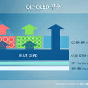
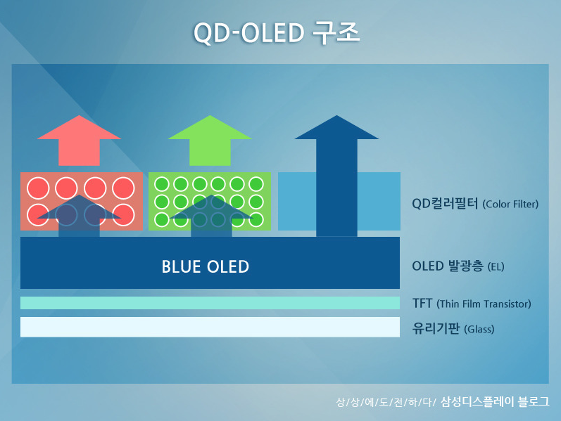
Recently, QD-OLED TV technology, which uses blue OLED as a light source and that implements red and green colors through a quantum dot color filter (QDCF), is attracting attention.

<Expected structure for QD-OLED, Source: Samsung Display Blog>

By using QDCF, it is possible to easily make desired colors by adjusting the size of the QD material and improve the color reproduction rate. This is because the color gamut is enlarged to BT2020, so it is close to natural color and it is possible to deliver vivid picture quality more clearly. In addition, QD-OLED TV has a top emission structure, which makes it easy to secure the aperture ratio, thereby improving resolution and screen uniformity.

However, in QD-OLED TV, there are various problems to be solved such as lifetime and efficiency of blue OLED, and technology of ink-jet printing process. Given that the industry is still in the early stages of reviewing the business possibility, QD-OLED TVs are expected to go into mass production after 2020.

Attention is focused on the QD-OLED TV’s entry into the premium TV market and its impact.

V-technology, announces acquisition of Lumiotec, OLED lighting company, and establishment of new subsidiary to develop next-generation OLED mask and deposition technology

V-technology said on February 7 that it would establish an ‘organic electronics business demonstration facility’ in Yonezawa, Yamagata Prefecture to develop a fine hybrid mask (FHM), which is next-generation deposition mask for OLEDs, and next-generation deposition technology.  The total investment is planned to be about 5 billion Japanese yen for two to three years. The facility is scheduled to be completed in August, 2018 and the mask samples are to be shipped from October, 2018.


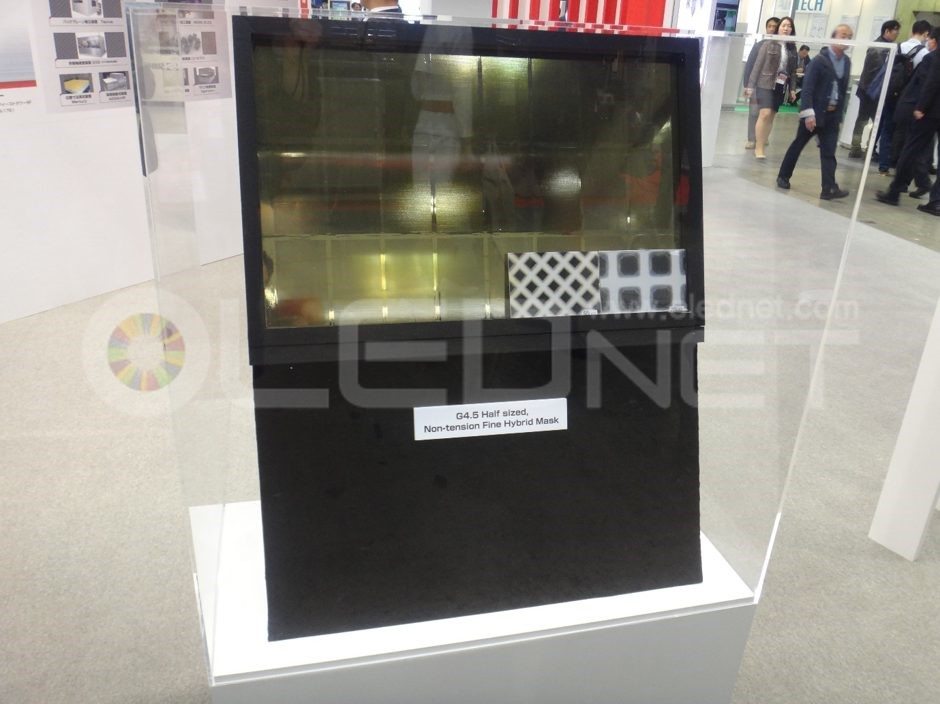
V-technology’s FHM adopts electroforming method and non-tension structure which is different from conventional FMM manufacturing method. The weight of the mask produced by this FHM method can be reduced to one tenth (1/10) level compared to the existing conventional mask. As the weight decreases, the problem of mask bending due to its own weight and shadow interference problem caused thereby can be solved. V technology already unveiled a Fine Hybrid Mask (FHM) that can implement 738ppi UHD at Finetech Japan 2017 in April 2017.

<V technology, Fine hybrid mask with non-tension structure>

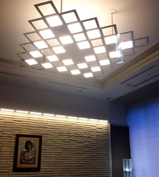
V-technology also announced that it has reached a basic agreement to transfer the entire stock of Lumiotec, a lighting OLED panel company. Lumiotec is specialized in lighting OLED panels in Japan, and has supplied a large number of OLED lighting panels for indoor use and exhibition use in addition to indoor lighting.

<Lumiotec lounge lighting, Source: Lumiotec>

V technology expects Lumiotec’s technology and business know-how to contribute to the group’s development. The stock transfer is scheduled for April, and information such as the transfer price is not disclosed.

RGB ink-jet printing, also applied to small and medium-sized OLED?

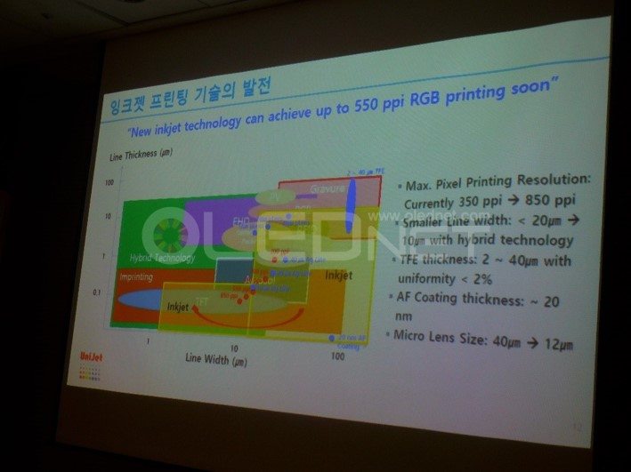
At the “Year End Seminar of OLED/Display” held at COEX in Seoul, Korea, on December 7, Kim, Seok-Soon, CEO of Unijet said that ink-jet printing technology can implement over 550 RGB ppi and ink-jet printing can be applied to small and medium-sized OLED process as well.

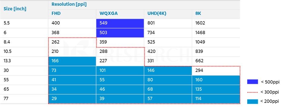
The currently mass-produced QHD resolution of 5.5-inch mobile device is 550 ppi but it is actually 400 ppi with pentile structure. Moreover the ink-jet printing technology for RGB pixels is currently in the range of 150 to 200 ppi which can achieve 8K resolution on over 55inch OLED, yet inapplicable to the small and medium-sized OLED process. As Kim announced, if the ink-jet printing technology is applicable, implementing 550 ppi in the small and medium-sized OLED process, beyond QHD resolution in 5.5 inches, it is possible to implement UHD resolution in pentile structure.

<ppi by size and resolution>

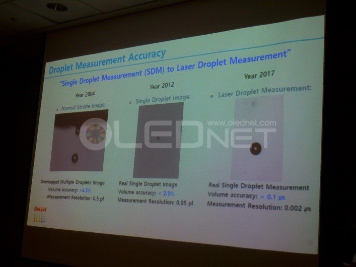
Kim said, “In 2012, single droplet measurement technology showed 2.5% or less of volume accuracy, which was, however, insufficient for RGB printing.  In 2017, the laser droplet measurement technology enabled the discharge volume control less than 0.1 μm and the real-time internal pressure control reduced the volume accuracy by less than 0.1%.” Kim added that it is possible to form over 550 RGB ppi regardless of the pixel structure.

Lastly, Kim noted that the solvent purity for OLED RGB pixel is very important; “Inkjet printer can be commercialized only if ink materials are fully developed first to satisfy panel makers. He expected that it will be applied to the mass production line in earnest since 2020. ”

[iMiD 2017] JOLED announces printing-type OLED development trend and future road map

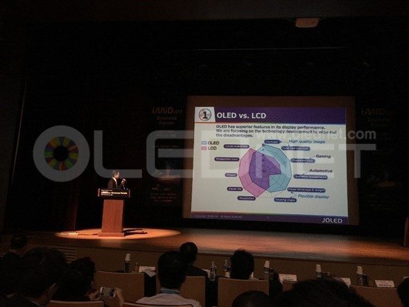
At the ‘IMID 2017 Business Forum’ held in COEX, Seoul from 18th to 19th, Toshiaki Arai, chief technologist of JOLED announced JOLED’s printing technology and future road map.

<JOLED’s Toshiaki Arai chief technologist>

Toshiaki Arai, chief technologist stated that a stable jetting technology at 220 ppi level has been currently secured; high resolution OLED with more than 300 ppi has been developed at Gen 8.5 but there are some issues such as jetting accuracy and stability.

Toshiaki Arai introduced TG-TAOS (top gate-transparent amorphous oxide semiconductors) TFT, which will contribute to saving the unit cost of OLED with excellent performance at low price.

He also announced the future strategy of JOLED, stressing that, instead of small and large OLED dominated by South Korean companies, the middle-sized OLED for tablet and monitor with more than 200 ppi. Joled is the only OLED panel maker that unveiled its 21.6 inch 4K RGB OLED in 2017, using printing process, and has pilot launched.

<JOLED’s 21.6 inch 4K OLED in application of printing method>

On the other hand, according to the Nihon Keizai newspaper in Japan, JOLED is reported to have invested 100 billion yen in mass production of printing-type OLED. In addition, Toshiaki Arai stated that the OLED test samples manufactured by printing process have been provided since this April and the mass production will realize in the second half of 2018.

Is there possibility of High resolution(UHD) OLED Smart-phone generation?

Recently VR contents experience through smart-phone device has been increased, therefore high resolution of smart phone is becoming necessary. However, OLED smart-phone resolution still remains at QHD level for 3 years since QHD OLED is applied to Galaxy Note 4 for the first time in 2014.

The core point that decides resolution of OLED smart-phone is evaporation process for emission layer. Bottom-up type evaporation method, which is applied to the recent devices is that substrate and FMM (fine metal mask) are horizontally arranged on the upper side of evaporator and vaporize the organic material from the lower linear source in order to form RGB layer.

Thin FMM measures less than 15um thick is necessary for making high resolution OLED like UHD level, however, as FMM gets thinner, it would be difficult to make mass production because technical problems will be occurred such as patterning, sealing and welding.

In order to solve these problems, various metal mask patterning technologies are being developed such as vertical type evaporation and plane source evaporation.

Vertical type evaporator that arranges board and FMM vertical is developed by Hitachi of Japan for the first time. And Canon Tokki exhibited Gen6 vertical type evaporator at Finetech Japan 2013, however it is not being used for mass production at the moment.

<Canon Tokki’s Gen6 vertical type evaporator which is exhibited at Finetech Japan 2013>


According to the recent ETNEWS, Applied Materials developed Gen6 flexible OLED vertical type evaporator and it is being tested in Japan Display.

Plane source evaporator is being tested but also the linear source type. Plane source evaporator method is that an organic material is first evaporated on the metal surface to produce plane source, then re-evaporated in order to form an organic thin film on the substrate.

In the past iMiD 2017, representative of OLEDON, Chang Hoon Hwang mentioned that 2250 ppi resolution OLED can be implemented through plane source evaporator.

For metal mask patterning technology, electro forming and laser patterning technology is highlighted. Electro forming method is developed by Wave Electronics, TGO Technology, Athene and so on. Laser patterning technology is being developed by AP Systems.

As such, development for high resolution OLED is receiving great attention whether it can solve the current problems and contribute to UHD resolution implementation for OLED smart-phone.

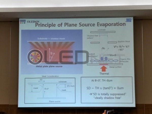
<Principle of plane source evaporation developed by OLEDON>

Cynora, TADF will contribute to high-resolution implementation of OLED devices and panel cost reduction

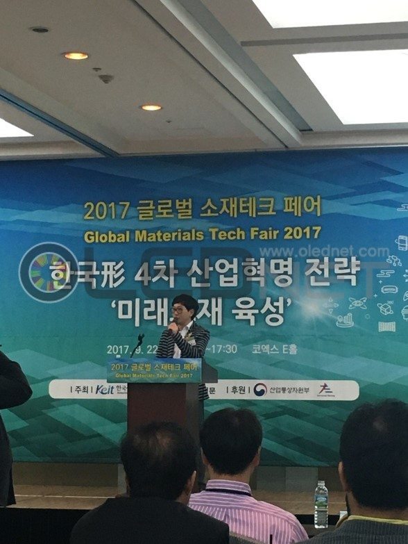
At the Global Materials Tech Fair 2017 held on September 22 in COEX, CEO Ko Chang-hoon of EM Index, Cynora’s Korean partner, announced the development of the thermally activated delayed fluorescence, blue TADF, which is currently under development at Cynora.


<CEO Ko Chang-hoon of EM Index>


Generally, the blue light emitting material is insufficient in life and efficiency compared to red and green. For this reason, OLED panels for mobile devices are manufactured relatively large in blue pixel size compared to other pixels, in the OLED panel for TV, blue light emitting layers are laminated twice. The blue TADF is the material that is being developed to overcome the limitations of this blue light emitting material.

CEO Ko Chang-hoon mentioned “Applying blue TADF increases lifetime and efficiency, so it does not need to increase pixel size and it is advantageous for high resolution implementation” and emphasized “In mobile devices, it will be advantageous to reduce power consumption as well as realize high resolution and in case of TV, it will be advantageous to reduce the panel cost because only one layer of blue light emitting layer needs to be formed.”

He referred to the recent investments of € 25 million from Samsung Venture Investment and LG Display and explained that it was a proof that blue TADF is attracting a lot of attention.

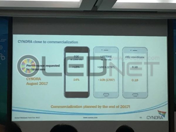
It is also close to the efficiency, lifetime and color purity of the blue TADF required by major OLED panel makers and is expected to meet these requirements by the end of 2017.


<Cynora’s blue TADF development progress>


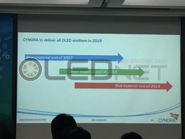
Finally, the company announced the development roadmap for the green TADF by the end of 2018 and the red TADF by the end of 2019, and concluded by emphasizing that TADF would contribute to high-resolution implementation of OLED products and panel cost reduction.

<Cynora’s TADF product development roadmap>

AUO unveils round OLED and foldable OLED for the smart watch in Touch Taiwan 2017.

AUO showed the OLED that can be collapsible and three kinds of round OLEDs (1.2-inch, 1.3-inch, 1.4-inch) for the smart watch in Touch Taiwan 2017 held on 20th.

The round OLEDs in 1.2-inch and 1.4-inch of AUO are 326ppi, and it lowers an electric consumption at 30% versus former production goods. AUO also improves the visibility capacity in outdoor by embedding the brightness increase mode to make a display screen of two kinds of round OLEDs be clear even under bright sunlight.

The 1.3-inch OLED aimed at the smart watch for kids is light in weight, and strengthens the usability with a power saving mode and an intuitive touch interface function.

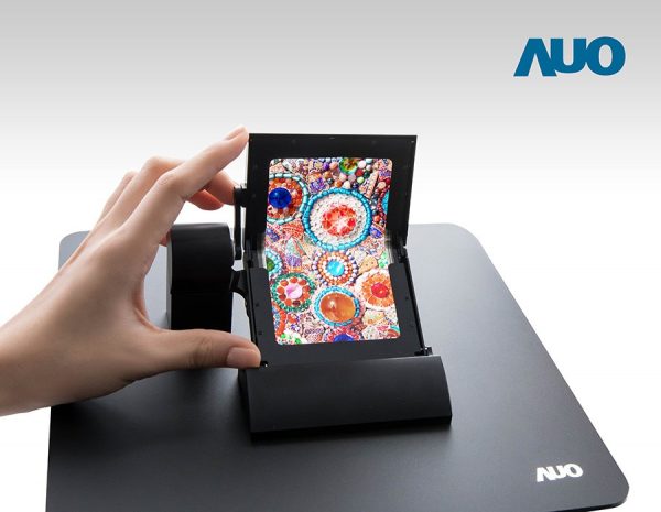
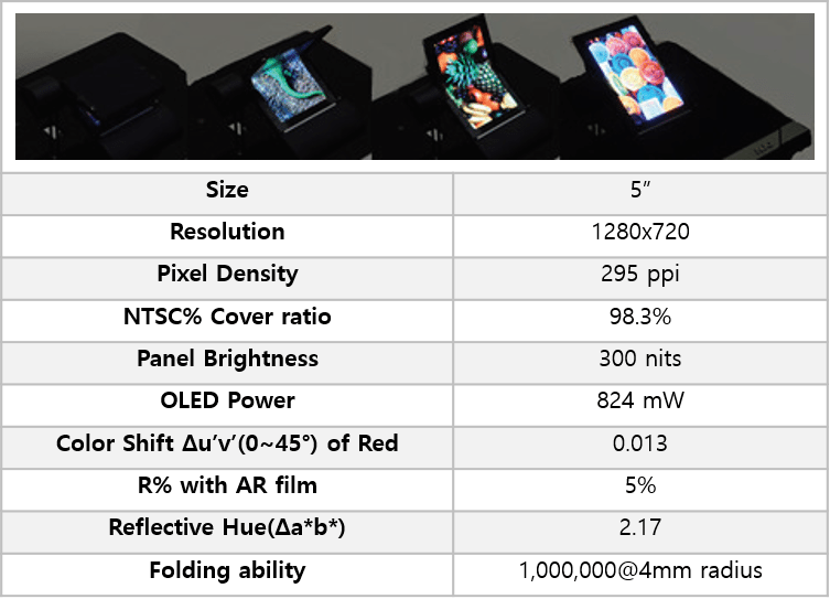
AUO displays two types of 5-inch flexible OLEDs that can be rolled or folded. Such two types of 5-inch flexible OLEDs apply the plastic board and AUO self-developed structure (special structural layer).


<AUO, 5 inch foldable OLED touch panel>


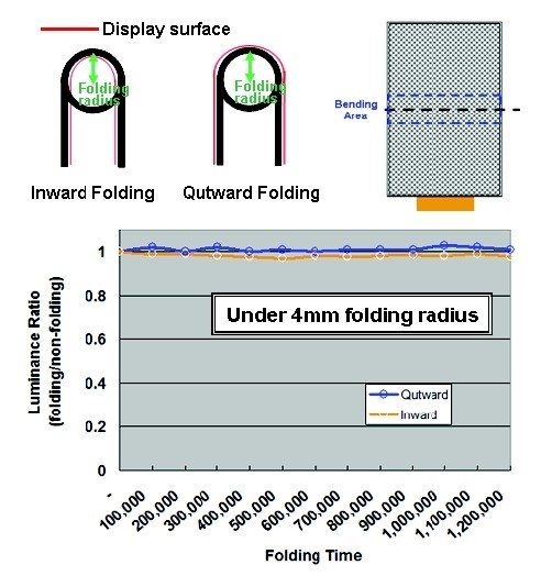
The 5-inch foldable OLED combines a flexible touch screen sensor that is developed by AUO itself.  The company said “it would provide excellent image quality, even if the curvature radius of the folded part is 4mm and less”.

For 5-inch rollable OLED, they explained “The thickness of the panel is just 0.1mm and only 5g. This model with the rolling radius of 4mm will provide wide color gamut”.

In last SID 2017, AUO has announced about that they applied the structure locating the TFT (Thin Film Transistor) and TFE (Thin Film Encapsulation) at the neutral axis to stand the compression stress or tensions during being folded.

Material Science to develop blue dopant for OLED … OLED Efficiency ⋅ Lifetime Up↑

A Korean venture company has succeeded in developing blue dopant for Organic Light Emitting Diodes (OLED) that a Japanese company has had its exclusive patent for. The dopant is an element that improves efficiency and life time by mixing with host that actually colors within the OLED.

In the meantime, many domestic material companies have developed OLED host, but it is the first case that a venture company has independently developed dopant on a commercial scale without receiving any support of large corporations.


Material Science (CEO Lee Soon-chang), an organic material developer for OLED has developed a technology that can replace Japanese I Company’s patent for blue dopant. Established in 2014, Material Science is supplying HTL( Hole Transporting Layer) and ETL (Electron Transfer Layer) to OLED panel makers.
Half of the 50 employees are R&D personnel. Last year, its sales were 6.6 billion won, and it is expected to exceed 10 billion won this year.

This time, due to the development of blue dopant by Material Science, OLED panel companies have an alternative to supply blue host and dopant besides I Company.

Japanese I Company has been developing blue dopant since 1995. At present, the company has more than 30 patents related to blue dopant (based on Japanese application for a patent), and its major 8 patents are valid until 2034. In particular, it has an exclusive patent for the combination method of blue dopant that includes blue host and pyrene with an anthracene structure (a compound in which three benzene rings are sequentially bonded). For this reason, the panel makers which purchase dopant from I Company must buy its host. If they mix I Company’s blue dopant with another company’s host, it is inevitable to infringe the patent in the case a host material has an anthracene skeleton.

Both Samsung Display and LG Display have been using I Company’s blue dopant and host.

The blue dopant developed by Material Science is designed to make molecules that are completely out of I Company’s compound patent. Conventionally, the method of applying an electron acceptor to a molecule has been used to improve the efficiency and lifetime of OLED and have a blue color.
On the other hand, Material Science introduces electron donor into molecules to improve the efficiency and lifetime while generating dark blue color. This dopant greatly reduces the solvent-dependent color development (solvatochromism) where emission wavelength changes due to the polarity of the surroundings. Therefore, the change of emission wavelength is also greatly reduced.

Jung Jae-ho, a researcher at Material Science said, “We have developed a new structure and a synthesis method, which makes it possible to produce its differentiated dopant.” “Panel companies are now able to utilize various types of blue hosts”. In addition, Material Sciences has been recently developing TADF(Thermally Activated Delayed Fluorescence) that OLED panel makers are struggling to introduce for the longer life of blue-emitting phosphors.


<OLED emitting material market forecast, UBi Research>

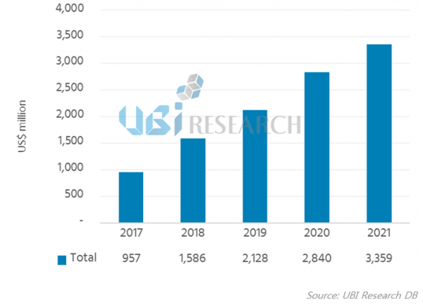
According to UBi Research, the OLED organic market is expected to reach $ 3.36 billion by 2021 (about 3.8 trillion won). And blue materials account for 11.5% of total sales.


[iMiD 2017] Samsung Display, Huge release of application using OLED

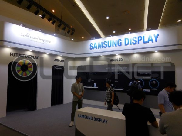
Samsung Display has received great attention by releasing a large number of applications using OLED such as VR and light field display in iMiD 2017 held in BEXCO, Busan from 28th to 31st August.


<Samsung Display booth>


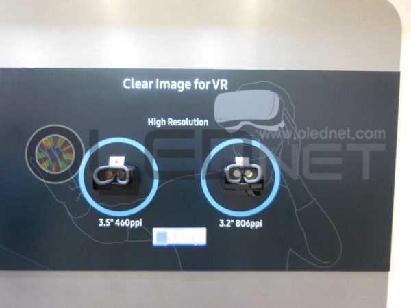
First, Samsung Display comparatively exhibited a 3.5-inch OLED with 460ppi resolution for virtual reality and an 806ppi 3.2-inch OLED. A company official said “The higher the ppi, the better the experience of realism and immersion,” and mentioned “We are currently developing higher resolution OLEDs.”


<Comparison of 3.5 inch 460 ppi OLED and 3.2 inch 806 ppi>


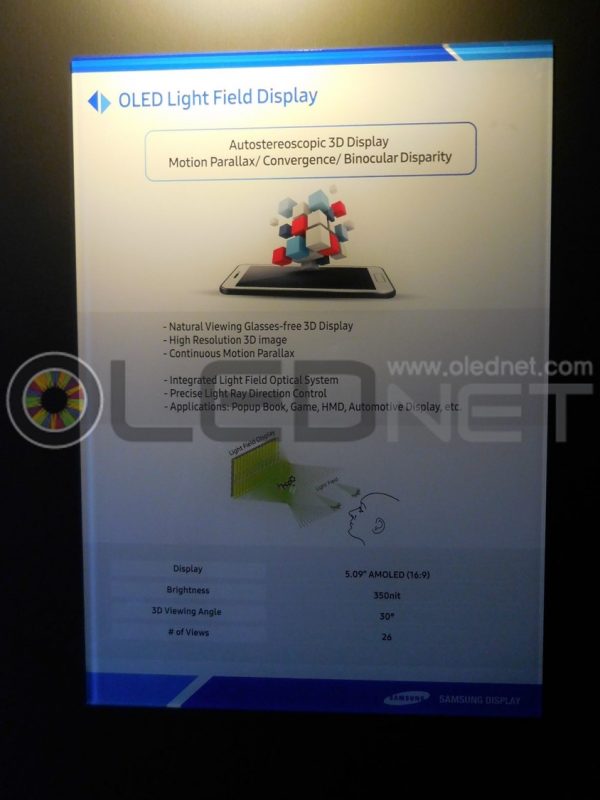
In addition, Samsung Display exhibited OLED light field displays in the future display zone, and in the AMOLED zone, visitors can directly compare LCD and OLED.

A company official explained that “light field display is a technology that implements 3D by applying an optical lens on a panel, which is a little different from hologram using light interference effect.” And he said “We are developing a viewing angle that is wider than 30 °,” revealed “We now have pixel and lens alignment issues and optical design issues.”


<OLED light field display description and specification>


In the AMOLED zone, panels were displayed to directly compare the contrast ratio of LCD and OLED. The contrast ratio and color expressiveness of the OLEDs were clearly different from those of the LCDs, and a company official said, “These differences are the reasons why OLEDs are used in the Galaxy series.”


<Comparison of OLED (Left) and LCD (right) image quality>


Samsung Display has also introduced 1.3 inch circle OLED and 12 inch FHD OLED, which led to the great interest of the visitors during the exhibition.

[iMiD 2017] LG Display, Spur Development of 77 inch transparent flexible OLED

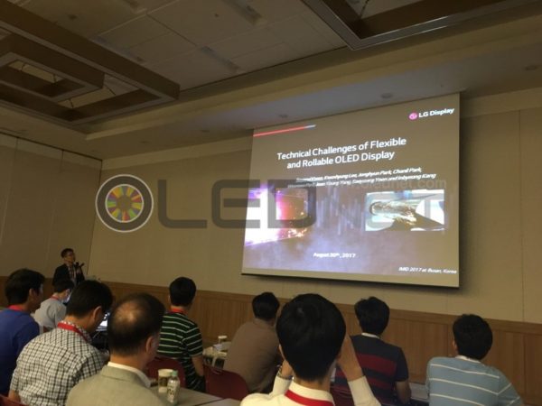
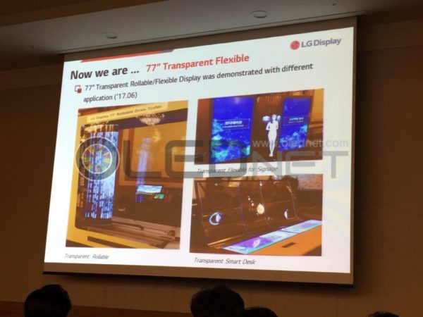
LG Display’s Kwon Se-Yeol senior researcher introduced the 77-inch transparent flexible OLED which had been introduced in June at IMID 2017 held in BEXCO, Busan on Aug. 30, and announced the applied technologies to realize this.


Kwon Se-Yeol senior researcher mentioned, “OLED is self-luminous, so it can be manufactured with a thin thickness because it does not need a back light unit. The thinner the thickness, the more flexible the OLED can be so that it is easy to implement flexible displays with OLEDs.” and forecasted. “It can be used in various fields such as signage and smart desk.”


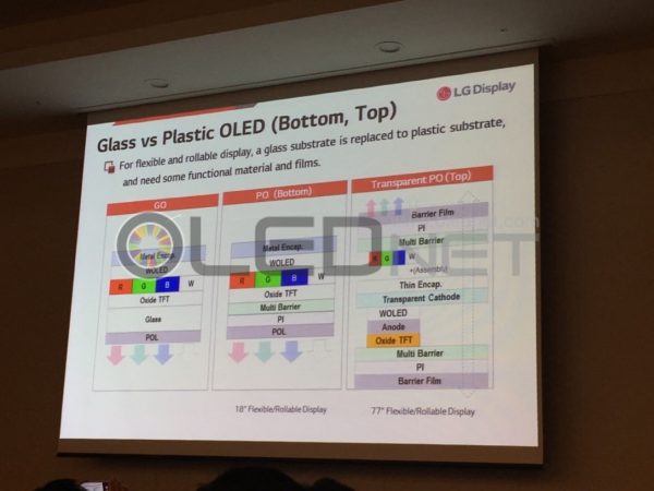
The 77-inch transparent flexible OLED which is released this time is a top emission type for improved luminance. The transparent thin film encapsulation layer is applied, different from the conventional OLED TV or large flexible OLED, and two polyimide substrates are used.


Kwon Se-Yeol senior researcher said “We applied a transparent thin-film encapsulation layer instead of the existing metal encapsulation layer for the top emission method ” and explained “A white OLED light emitting layer and a color filter layer were formed on two polyimide substrates and cemented together. A barrier film and a multi-barrier were applied to the top and bottom of the polyimide substrates to prevent moisture and oxygen penetration.”


The Kwon Se-Yeol senior researcher then states that “flexural rigidity of the panel is mainly affected by the thickness of the polarizer and the encapsulant layer, so it is necessary to reduce the thickness in order to improve the flexibility”, and emphasized “By reducing the thickness of the encapsulant layer from 100 μm to 20 μm, we can reduce the strain on the OLED module from 0.36% to 0.21%, along with improved flexibility”.

In addition, he mentioned that surface reflection due to polyimide birefringence phenomenon, laser wavelength selection according to polyimide properties in LLO (laser lift off) process, and use of flexible OLED module are all covered, and technical development is continuing.

Meanwhile, LG Display has developed the world’s first 77-inch transparent flexible OLED with UHD (3840 × 2160) resolution, transmittance of 40%, and radius of curvature of 80R as part of the national project.

[iMiD 2017] OLEDON, 2250ppi OLED제조용 면소스 FMM 증착 원리 공개

28일 개최한 iMiD 2017에서 단국대학교의 실험실 벤처 OLEDON사 대표 황창훈 교수는 2250ppi를 구현할 수 있는 면소스 FMM 증착 기술에 대해 발표하였다.

황창훈 교수의 발표에 따르면, OLEDON에서 개발한 면소스 증착 기술은 기존 유기물 증착 방식과 다르다. 면소스 FMM 증착 기술은 유기물을 금속면에 1차로 증착하여 도너 박막을 형성하고 면소스를 만든 후, 이를 재 증발시켜 기판에 유기물 박막을 형성하는 원리이다. 이 기술을 적용하면 유기물은 면증발로 인해 수직성 기체빔을 형성하게 된다. (원천특허:1012061620000 대한민국)

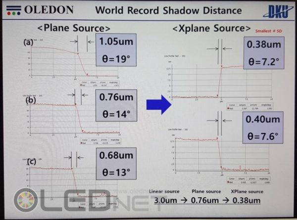
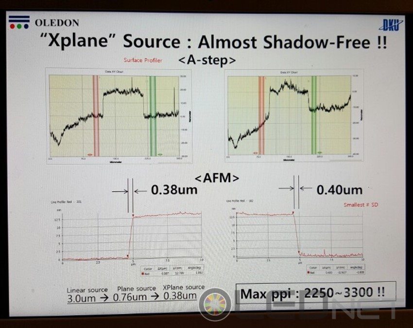
OLEDON사가 개발한 면소스로 유기물을 증착 했을 때의 섀도우 거리는 0.38 um – 0.59 um이다. 이는 4 um의 패턴 사이즈를 가지는 2250ppi 소자를 제작할 수 있는 수준이다.

황창훈 교수는 ‘면소스 증착 기술을 적용하면 유기물 기체의 입사각이 줄어들어 마스크에 의한 섀도우 현상을 획기적으로 줄일 수 있다’고 설명했다. 또한, ‘면소스는 수직성 유기물 기체빔이 완전 제로 입사각을 형성할 수 있어 이론적으로 섀도우 거리가 제로 um도 가능하다’고 덧붙였다.


<OLEDON사가 개발한 면소스 증착 기술 원리>


또한, 이번 발표에서 황창훈 교수는 ‘면소스 증착기술은 고해상도용 섀도우마스크의 제작에도 필수적’이라 강조했다.

현재 양산에 적용중인 리니어 소스 FMM의 경우 섀도우 마스크의 오프닝간 거리는 80um이다. 이로 인해 유기물 기체빔의 입사각은 커질 수 밖에 없어 고밀도 패턴을 가지는 섀도우 마스크 제작이 어려운 실정이다.

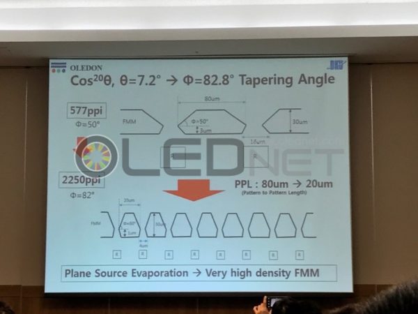
황창훈 교수는 ‘면소스 증착 기술을 이용하면 섀도우 마스크의 테이핑 각도는 80° 수준이다’며 ‘오프닝간 거리를 20 um미만까지 줄일 수 있어 면소스 증착 기술은 리니어 소스가 가지는 마스크 패턴 밀도 문제를 해결할 수 있다’고 설명했다.

OLEDON사는 면소스 증착 기술로 완전 shadow-free 패터닝 조건에 도전하고 있으며, 단국대학교의 진병두교수팀과 공동으로 11K급 마이크로 OLED 소자의 제조가 가능한 면소스 FMM 증착기를 단국대학교내에 개발 설치할 계획이다. (참고:OLEDON사의 홈페이지 www.oledon.co.kr)


<면소스 FMM 증착기술을 사용시 섀도우마스크의 오프닝밀도 변화>


한편, OLEDON사은 양산용 면소스 FMM 증착기에 대한 13건의 등록특허를 보유하고 있다. 최근 연구 결과를 토대로 양산장비 신규특허 7건을 국내출원 하였으며, 3건을 PCT 국제출원 중이다.

[iMiD 2017] OLEDON, Disclose plane source FMM deposition principle for 2250ppi OLED manufacturing

Prof. Hwang Chang-Hoon, CEO of OLEDON, a venture laboratory of Dankook University, presented a plane source FMM deposition technology capable of implementing 2250 ppi at iMiD 2017 held on the 28th.

According to Prof. Hwang Chang-Hoon’s presentation, the plane source deposition technology developed by OLEDON differs from the existing organic material deposition method. The plane source FMM deposition technique is that the organic material is first deposited on the metal surface to form a donor film and then re-evaporate it to form an organic thin film on the substrate. Applying this technique, organic matter forms a vertical gas beam due to plane evaporation. (Source patent: 1012061620000 Republic of Korea)

The shadow distance when organics are deposited with a plane source developed by OLEDON is 0.38 μm – 0.59 μm. This is a level at which a 2250ppi device having a pattern size of 4 um can be manufactured.

Prof. Hwang Chang-Hoon explained ‘applying the plane source deposition technique reduces the incidence angle of the organic material and dramatically reduces the shadow caused by the mask’. In addition, ‘using a plane source, the perpendicular organic gas beam can form a completely zero incident angle, so theoretically, the shadow distance can be zero um’.


<Principle of plane source deposition technology developed by OLEDON>


In addition, Prof. Hwang Chang-Hoon emphasized that ‘plane source deposition technology is essential for high-resolution shadow masks’.

For linear source FMMs currently in production, the shadow mask opening distance is 80 μm. As a result, the incidence angle of the organic material gas is inevitably large, making it difficult to produce a shadow mask having a high density pattern.

Prof. Hwang Chang-Hoon explained, ‘Using plane source deposition technology, shadow mask taping angle is 80 ° level’, and the distance between openings can be reduced to less than 20 μm so that plane source deposition techniques can solve the mask pattern density problems of linear sources’.

OLEDON is challenging fully shadow-free patterning conditions with plane source deposition technology, and plan to develop and install a plane source FMM evaporator capable of manufacturing 11K class micro OLED devices in cooperation with Prof. Jin Byung-Doo in Dankook University. (Reference: Homepage of OLEDON www.oledon.co.kr)


The opening density change of the shadow mask when the plane source FMM deposition technique is used


Meanwhile, OLEDON has 13 registered patents for plane source FMM deposition for mass production. Based on recent research results, they filed 7 new patents for mass production equipment in Korea and 3 applications are filed for PCT international application.

[iMiD 2017] AP Systems, Find FMM answers through USPL

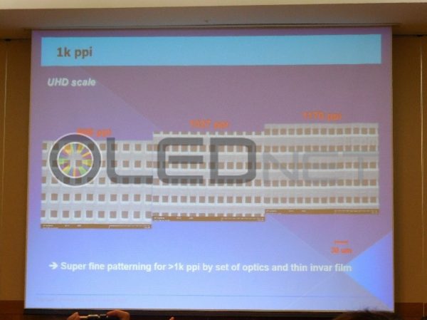
At iMiD 2017 in BEXCO, Busan on 28th, AP Systems announced that it succeeded in developing 1000ppi FMM with USPL (ultra-short pulse laser).

Since FMM plays a role of depositing pixels and RGB organic materials, FMM serves as a factor that determines resolution and yield of OLED. At present, FMM is mainly manufactured by etching method. This method has a problem that a shadow phenomenon due to the precision, thickness, and weight of the fine pattern occurs, in order to solve this problem, various FMM manufacturing processes such as laser processing and electro-forming have been developed.

Among these, laser processing method has an issue of forming burrs around pin-holes due to the thermal effect caused by laser irradiation. These burrs increase the shadow interval of the FMM, which causes overlapping of patterns during RGB organic deposition, thereby degrading the resolution of the OLED.

AP Systems has developed a burr-free laser process that does not have burr phenomenon and further controls the taper angle.

The Burr-free laser process is a short-time irradiation of unidirectional pulses at a constant number of times, since the laser is not continuously irradiated, it minimizes accumulated heat energy and prevents burr formation. In addition, by controlling energy of the laser, it accumulates energy and forms taper.

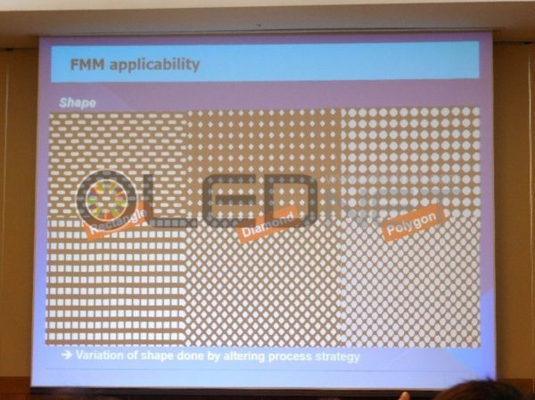
In this way, AP Systems explained ‘they produced FMM with various shapes of fine pin-holes such as square, diamond, and polygonal shapes, as well as 1170ppi FMM’, and ‘’We also developed large-area FMM manufacturing equipment with USPL method’.

AP Systems also added ‘multi-beam and USPL is equipped for FMM manufacturing equipment so that it can improve productivity and realize UHD’.

Since the launch of the Galaxy Note4 in 2014, the OLED resolution has remained at the QHD level yet. In order to manufacture an OLED having a high resolution (UHD level or higher), it is necessary to solve various technical problems faced by FMM. Accordingly, it is noteworthy how USPL technology of AP Systems will affect the future OLED market.

<1000ppi FMM produced by AP Systems>


<various type of FMM produced by AP Systems>

[iMiD 2017] TCL, Development focusing on Solution process OLED and QLED

TCL’s Xiaolin Yan CTO addressed solution process OLED TV and self-emitting QLED TV as premium TV after white OLED TV at iMiD 2017 keynote address in BEXCO, Busan on 29th.


Yan CTO noted that white OLED TV, which is currently leading the premium TV market, meets all the requirements of premium TV due to its superior image quality, design differentiation, high resolution realization and nature-friendly characteristics compared to QD LCD TV.


In addition, the price that is higher than the current QD LCD TV is expected to be overcome by applying the solution process, and mass production is also expected in 2019.


Yan CTO predicted that the “solution process would be easy to produce 75-inch panels at Gen 10.5 because the process can be performed without splitting the ledger,” and “it is also possible to produce full-emission RGB OLED TVs.” However, he emphasized that the compatibility of materials and equipment and the development of ink forming process technology should be done.


Following to that, “QLED structure is very similar to OLED structure, so it is easy to apply the technology because of the low entry barriers,” he said. “The lifetime and efficiency of the blue light emitting layer compared to the current OLED is very low, and performance must be ensured without the use of cadmium.”


Lastly, He mentioned the establishment of printing technology in Guangdong JUHUA to promote the commercialization of solution process OLED TV and self-luminous QLED TV, and emphasized the cooperation of material, equipment and panel makers to develop next-generation premium TV.


Stretchable OLED commercialization is on the rise

Samsung Electronics and LG Electronics have steadily been releasing smartphones and smart watches using flexible OLED since 2013, and electronics companies in China have begun to put out one of them. In particular, Apple, the leader in the smartphone industry, is also seeing the launch of iPhone with flexible OLED, and the flexible OLED market is expected to grow further.

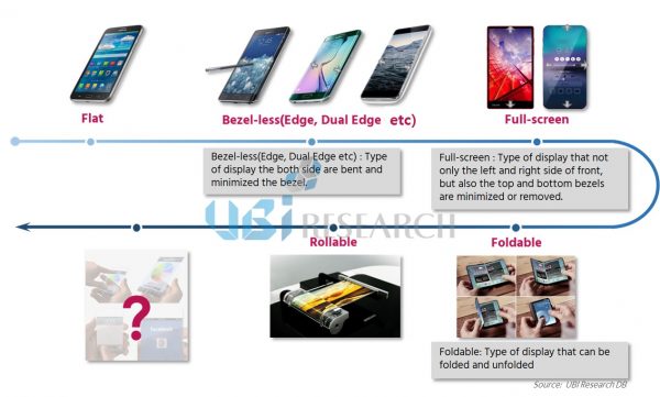
The shape of the flexible OLED was expected to be changed to foldable and rollable beyond the bendable. Recently, however, the display industry has surpassed this trend and has been focusing on the development of stretchable OLEDs.


<Development Roadmap of OLED, Source: Ubi Research>


A stretchable OLED is a type of a flexible OLED that is finally evolves, which means OLED having elasticity as like rubber band.


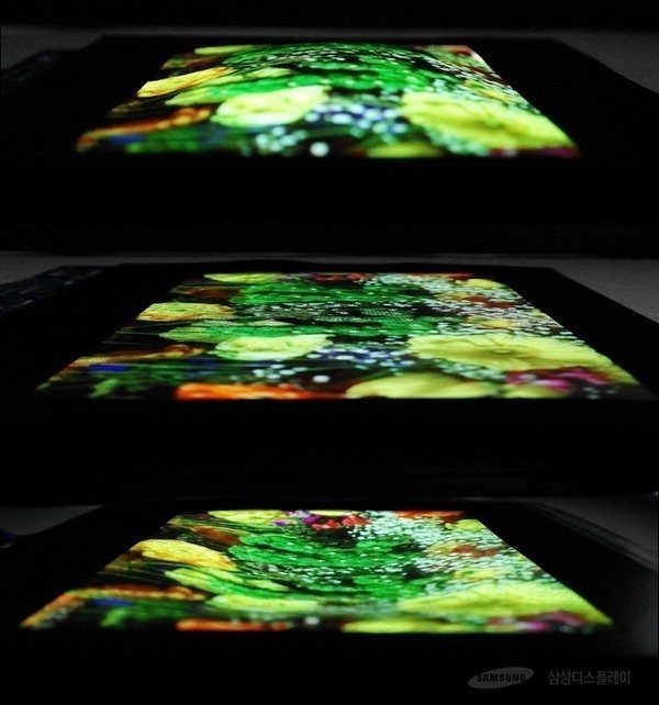
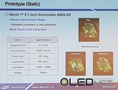
Samsung Display unveiled this stretchable OLED at SID 2017. Samsung Display’s stretchable OLED is 9.1 inch and implementable both convex and concave shapes. At the time, Samsung Display announced that it realized the world’s first technology to maintain the existing image quality while increasing the screen size to 12 mm in concave mode.


<9.1 inch stretchable OLED displayed by Samsung Display, Source: Samsung Display>


LG Display will also develop the stretchable OLED. LG Display announced on June 6 that it will develop backplane and photoluminescence materials, devices, and process source technologies with elasticity of more than 20% for a total of four years through a consortium with Korea University.


In addition, LG Display has developed flexible plastic substrate materials, flexible wiring materials and transparent electrode materials, stretchable organic light emitting materials, and flexible encapsulates, they will also acquire essential process technologies including thin film transistors (TFTs) and process architectures that enable low-temperature processing.


At present, stretchable related technology is not yet applied to production, or elongation is only about 5%, and the number of repeated stretching is limited. In addition, most of the source technology is in overseas, it is expected that Samsung Display and LG Display will be able to secure technological gap with latecomers.

Stretchable OLED is free of form restrictions and expected to produce applications in new areas when applied to a variety of applications such as smart phones, tablets clothes and human skin when they are commercialized.

Truly and FlexEnable sign License Agreement to bring low-cost, scalable flexible display production to China


31 July 2017 – FlexEnable, the leader in the development and industrialization of organic electronics for flexible displays and sensors, has signed a technology transfer and license agreement with Truly Semiconductors, one of the leading display makers in China. The deal aims to bring FlexEnable’s flexible organic liquid crystal display (OLCD) technology into mass production on Truly’s lines within 2018.


Due to its high performance and low cost manufacturing process, OLCD is the only display technology today that can deliver flexible displays with large area, low cost and high brightness with long lifetime. With a bend radius that can go below 20 millimeters, OLCD meets the market needs for a range of applications across consumer electronics, smart home appliances, automotive, digital signage and beyond.


OLCD is based upon FlexEnable’s flexible low temperature organic thin-film transistor (OTFT) backplane technology, which can be manufactured on existing TFT LCD production lines using low cost plastic substrates such as TAC and PET. The OTFT backplane has better electrical performance than amorphous silicon, giving plastic LCDs the same display quality and reliability as glass-based LCDs, while making it thinner, lighter, shatterproof and conformable to surfaces.


Truly, the first display manufacturer to adopt OLCD, will implement the process into its existing production lines in Shanwei, China. The first product samples will be available to commercial partners in early 2018, with volume production expected in late 2018.


Chuck Milligan, CEO of FlexEnable, says, “Truly is a leader in displays manufacturing and a top-level supplier of displays to key market segments to which FlexEnable’s technology can bring great commercial advantages. We are already working with brands who use OLCD in their product concepts and who now need access to a volume supply chain to realize some very exciting new product offerings with designs that simply aren’t possible with other types of display. We are excited that Truly has become the first display manufacturer to implement FlexEnable’s game-changing OLCD platform and meet market demand for flexible displays.”


KK Ho, General Manager, R&D center, Truly Semiconductors Ltd, says, ”FlexEnable’s OLCD technology is a breakthrough in the TFT-LCD industry and with its characteristics of thinness, lightweight, and more durability it is going to create lots of possibilities for innovative product design. We have been receiving many enquiries for flexible display from the market, specifically, wearable devices, smart home appliances, electric cars and self-driving cars etc. This is a pretty exciting display technology and we do believe there is a considerable potential market size.”


-ENDS-


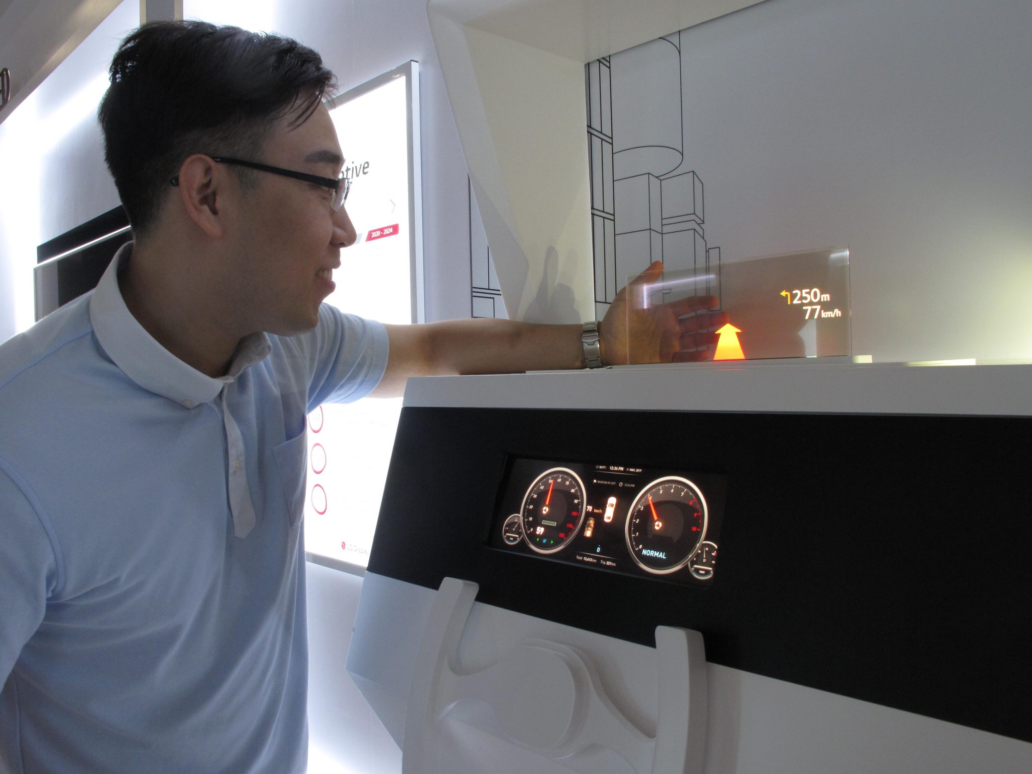
The OLED is the best automotive display

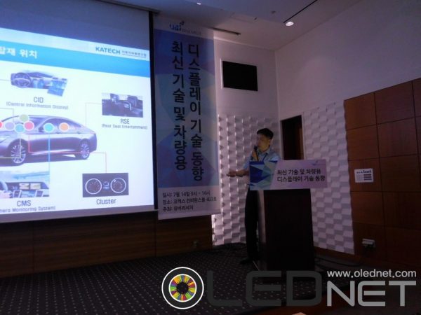
The seminar on the trend of the up-to-date technology for the next generation display which was themed ‘The technology trend for latest display and the automotive display’ hosted by the UBI Research, was held on July 14th at COEX in Seoul.


In the seminar, Sun-hong, Park, a senior researcher of automotive parts, said that “The attention to the display is increasing due to the importance of the visual intelligence, and its application will also grow because the OLED is able to easily realize the flexible deign and the transparent display.”

In addition, he expected that “The digitalization for the automotive will be lasting, and the China will take 50% and more of the worldwide consumption market for automotive in 2020, and the application of display including OLED will increase in accordance with the attributes of the Chinese who prefer colorful design.”

During the briefing of a car not having a side mirror which became an issue in recent, “The application of the OLED which has rapid response speed and wide viewing angle is highly likely to be employed. If it can just overcome the reliability, the OLED will be the best display for the automotive.”

In the other side, according to the “Automotive Display Report – application & market trend analysis and the market forecast” published by the UBI Research, it expected the OLED panel will be started in earnest applying to the cluster or CID of the automotive from 2018, and the automotive display is expected to grow about 17% annually, reaching around US$ 25,000 million by 2022. The AMOLED panel market among this will be account for about 20%.


<Forecasting of the market share by the automotive display 2017~2022>


LG and Samsung at the International TADF Symposium in Germany

TADF (Thermally Activated Delayed Fluorescence) is an exciting new technology to provide highly efficient and stable emitting materials for OLED devices. TADF emitters are poised to contribute to the next material-driven advancement of the OLED industry, making OLEDs ideal for even more applications. Right now, TADF technology is receiving much attention as it will lead to major improvement of OLED displays again. The importance of TADF technology and its impact of the Next-Generation OLEDs will be highlighted at the International TADF Symposium in Frankfurt, Germany. (www.tadf-symposium.com)


Directly after the well-known IFA conference, the world’s leading researchers from European and Korean universities will discuss aspects related to the development of TADF OLED materials from modelling through synthesis to analytics and device fabrication. In addition, the leading OLED manufactures LG and Samsung will reveal some of their views on the OLED industry and what impact high-efficiency TADF materials will have on it. Furthermore, CYNORA, the leading TADF materials provider, will present an update of its status and its finals steps in commercialization of first blue TADF emitters.

The registration for the International TADF Symposium will be open till 15th August. The TADF event is sponsored by Lesker Tool, Schrödinger and CYNORA.

Meet the leading experts from OLED industry and academia on September 7th in Frankfurt, Germany.

Reduce OLED manufacturing time to 1/10

Manufacturing technology has been developed to quickly fabricate OLED.
The Korea Research Foundation (KFRI) announced the Yun, Hongseok research team at Hanbat National University has developed a high-speed transfer technology that can effectively transfer multiple thin OLED layers to desired locations through high-pressure air jet injection.

The OLED transfer separates multiple layers of thin film from the substrate all at once and combines them with other thin films to produce a device. At this time, the thin film is ripped apart or wrinkled, and the corner is torn off, which make it difficult to mass-produce.


<A conceptual diagram of energy transfer process of polymer OLED multilayer thin film using air jet, Source: Korea Research Foundation>


The team used the principle of effectively controlling the bonding energy between the thin film and substrate by a high-speed peeling technique using the air jet technology,. An air jet close to the sonic speed is injected between the substrate and OLED thin film to effectively reduce the bonding force with the substrate, thereby enabling the transfer without damaging the thin film. The high-speed transfer method through the air jet requires only short time to transfer the OLED; the processing time takes about 1/10 of production time. OLED thin films can be manufactured at low cost by coating them with a solution.

Professor Yoon, Hongseok explained, “This research has developed a technology that can rapidly manufacture OLED device because they can be effectively transferred all at once by using an air jet without damaging the OLED thin film. The unit production cost of OLED can be significantly reduced, which has been used in a wide range of applications such as OLED lighting, advertising and display. It is expected to be applied to basic electronic devices in the future such as solar cells and semiconductor devices. ”

The research was carried out with the support of the Researcher Support Project for the Basic Research Support Program of the Korea Research Foundation and was published in the international journal on nanomaterials applications, Nanoscale.

OLED TV is the competitive TV covering the whole areas such as the design and the sound quality as well as the image quality.

“While the existing OLED TV is focused on the image quality, the current OLED TV is not only picture quality but also covering any areas including the design and the sound quality.”

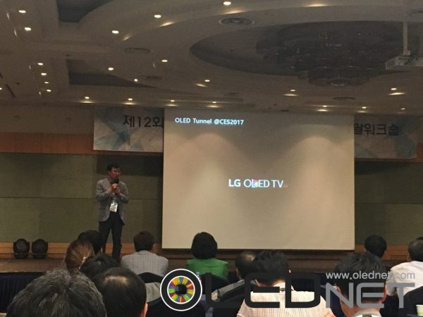
In the keynote address for the workshop of ‘the 12th Display National R&D Projects’ held on 5 July in Hoengseong, Gangwon-do, Soo-young, Yoon, a director of LG Display, introduced the advantages of OLED TV such as superior image quality, design freedom, and sound quality improvement including the capacity of the light and shade, and color implementation.


He said, “It is unlike LCD, OLED is the self-emitting, and be able to be controlled by a pixel unit, so that it is capable of expressing the perfect black, and implementing the unlimited contrast range. Therefore, OLED is the best display to express the stars or a bright moon in the darkness.” And also, he emphasized that “OLED TV is free to express the middle gradation through the precise color expressiveness, so that it is able to realize the vivid color as realistic.”


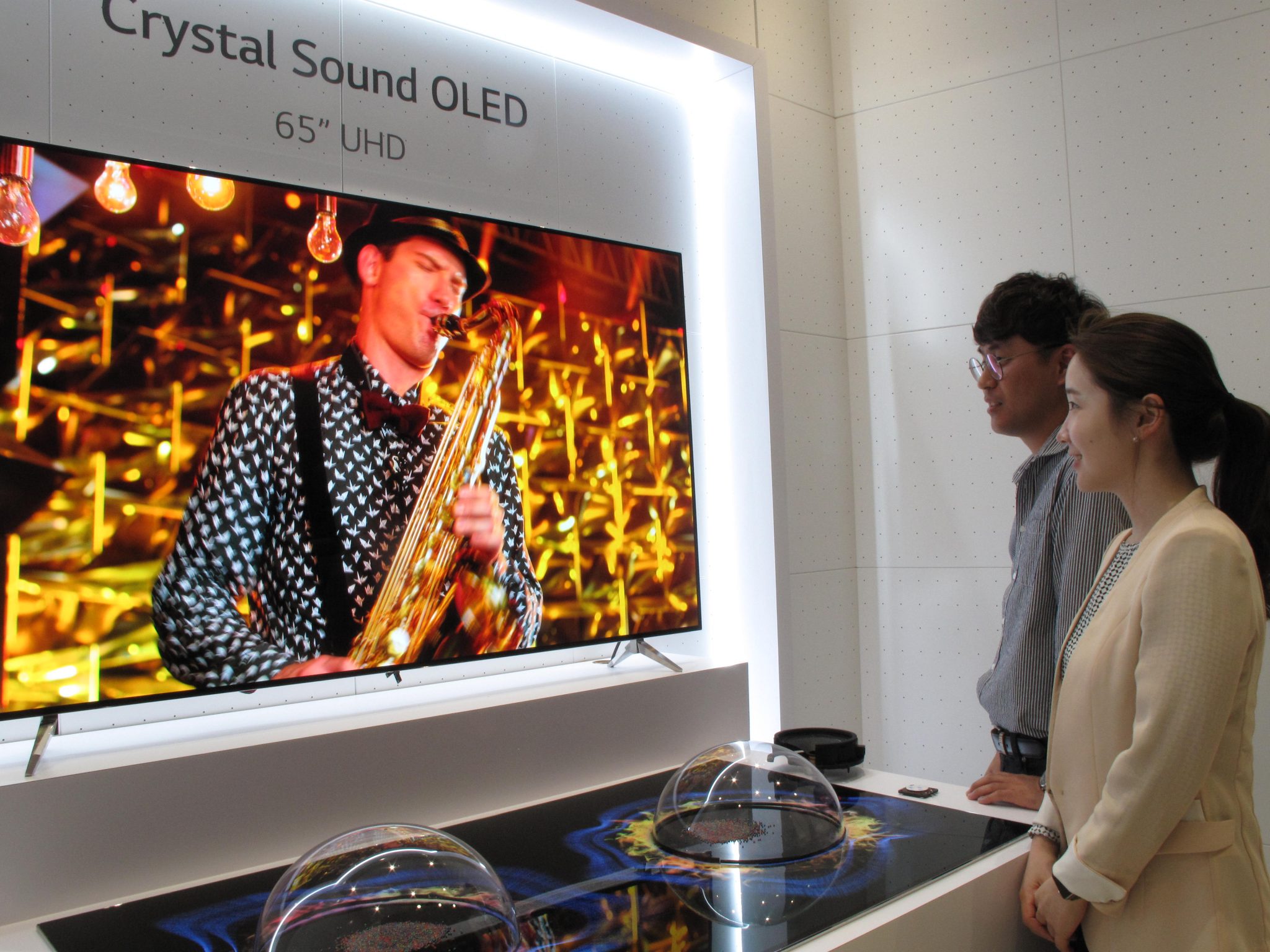
Subsequently, he introduced the wallpaper and CSO (crystal sound OLED) which attracted lots of attention in last CES 2017, “If the existing OLED TV is an image quality-oriented, the current OLED TV goes through any areas such as the design, sound quality but also the image quality. Especially, the embedded speaker methods are able to realize the high level of immersion, by agreeing the position of the mouth and the sound along with the effect of design advancement.”

A director, Soo-young, Yoon, also introduced the transparent flexible OLED which can implements the radius of curvature 80R, 40% penetration ratio, and 77-inch UHD, that developed for the commercialization, and mentioned that the transparent and flexible display will be a future display. He also said that they are on-going to develop the devices and materials for solution process, and it needs to be discovered the new application and new form factor.

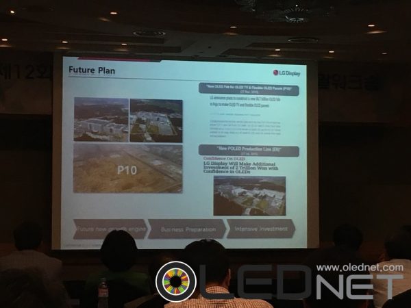
Finally, he mentioned the P10 factory at Paju, “We expect to ultimately produce new OLED TV at P10 factory which plans to be completed by the end of this year through thorough preparation.”


OLED Highly Polarized OLED, A New Approach to Improve OLED Light Efficiency,

Professor Kim Jae-Hoon of Hanyang University announced at the seminar, ‘OLED market analysis and latest technology’ for the first half, host by UBI industry research last June that a small amount of chiral molecule added to the polymer OLED emissive layer controls the polarization of light emission to improve light efficiency by 60%.


Two linear polarizers applied in orthogonal form to LCD are used to transmit or block the light from the back light unit through liquid crystal movement while one circular polarizer of OLED prevents reflection of external light, which is applied as a role to increase outdoor visibility

Display companies have focused on development of device structure, optical extraction technology and material, and luminescent mechanism to compensate for more than 50% luminescent light loss due to the polarizer. We need a way to improve the efficiency of OLED using polarized light. Professor Kim, Jae-hoon has presented a method and research results to improve the OLED light efficiency in use of polarized light, emphasizing ‘the need of a new approach in a new perspective’.


<Simulation of chiral molecules-added OLED structure>


Professor Kim, Jae-hoon explained, ‘Polymer materials of OLED generate high linearly polarized light with high liquid crystallinity in general. When this light passes through a light emitting layer inclusive of chiral molecules, it becomes a circularly polarized light’. “Theoretically, the light efficiency can be increased by 100%,” he added. “This way, we can implement brighter OLED with lower power consumption.”

In application of this principle, Professor Kim, Jae – hoon and his team members have developed the OLED with luminous efficiency 60% higher than existing OLED and further research will be continued on circular polarization based on low molecular materials.

Meanwhile, the research was sponsored by the ‘Future Display Core Technology Development’ project, and the research outcomes have been published in the recent issue of an international journal, ‘Advanced Materials’.

OLEDON, Find the future of AMOLED in plane source FMM!

Three years have passed since the first QHD (about 515 ppi) OLED applied to Galaxy Note4 in 2014, but OLED resolution is still in QHD. In order to manufacture high-resolution OLED over UHD, FMM of less than 15 μm is required, but it is not applied to mass production due to various technical issues.

Professor Hwang Chang-Hoon, CEO of OLEDON, a venture business of Dankook University, proposed that the plane source FMM deposition technology is the only solution for a high-resolution OLED manufacturing process over UHD at the 1H semester UBI Research Seminar “OLED Market Analysis and Latest Technology” held on June 30 (Fri) at Yeouido FKI Conference Center.

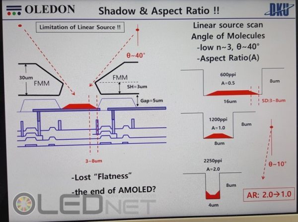
Professor Hwang Chang-Hoon said, “To improve the resolution of AMOLED, the angle of flight of organic molecules should be reduced to less than 10 degrees and the aspect ratio of TFT devices should be maintained at 1.0 level.” and explained “The evaporation angle (incidence angle) of the currently known linear source is about 40 degrees, and the shadow distance is about 3 um. Therefore, the ratio of the pattern width, the shadow distance, and the aspect ratio can be increased at the SUHD level AMOLED patterning process. Ultimately, the current patterning technology loses the flatness of the film. “.

In addition, Professor Hwang Chang-Hoon said, “Linear deposition technology has limitations in achieving resolution higher than QHD, and development of plane source FMM deposition technology is the only way to manufacture OLED with 2000 ppi or higher.”.


<Professor Hwang Chang-Hoon announced the 2250ppi AMOLED technical problem, Source: the 1H semester UBI Research Seminar>


The shadow distance measured by OLEDON’s plane source FMM deposition technique ranges from 0.68 to 1.05 μm and the angle of incidence is 13 to 19 degrees and converting this result to resolution makes it possible to fabricate a device with a maximum of 1500 ppi. On the other hand, with the newly developed Xplane source, the shadow distance was 0.38 ~ 0.56um and the incident angle was 7.2 ~ 8.0 degrees, it is possible to manufacture up to 3300 ppi device by converting it to the resolution. In the last SID2017, Prof. Jin Byung-Doo and Prof. Hwang Chang-Hoon introduced the world’s first measurement of sub-micron-scale shadow distance using plane source patterning technology, it has been announced that it is possible to manufacture a micro AMOLED device having a Super Ultra (SUHD) resolution of 11K (2250 ppi) or more if scale-up development is applied to large-area OLED display production industry in the future. (Paper title: Plane source evaporation techniques for Super ultra high resolution flexible AMOLED)


Sub-micron Shadow data and incident angle data obtained by plane source FMM deposition technology, Source: the 1H semester UBI Research Seminar


On the other hand, based on the development results, OLEDON announced that it plans to develop and install planar source FMM evaporator for research, which can manufacture ultra-high resolution micro OLED devices using plane source deposition technology, in Dankook University. (Refer to: OLEDON homepage www.oledon.co.kr)


UBi Research first half year closing seminar ” OLED Market analysis and latest technology”

OLED Market

■ Review the technical issues & market in the OLED industry in the first half of 2017

■ Market outlook and change points forecast for the 2H of the year thru 1H issue analysis


UBI Research will hold an OLED market analysis and latest technology on June 30 (Fri) at the FKI Conference Center in Yeouido, Korea, to finalize the OLED market in the first half of 2017 and forecast the market in the second half of 2017.


In this seminar, we will look at the investment trends and future of major panel makers and look at OLED market trends and latest technologies such as development status of luminescent materials of TADF and Iridium phosphorescent materials, technology issues for flexible OLEDs, and surface patterning deposition technology for high resolution so that it will be a place to preview how OLED markets and technologies will change.


In this seminar, (Kwon Seong-Ryul, head of Dongbu Securities Industry Analysis team will be presenting on changes in OLED portion in smartphones, TVs, and signage, and polarization of major OLED panel suppliers by country, forecasts of major OLED equipment and materials markets, possibility of foldable display and technical difficulties and etc.


Following this, Chang Jung-Hoon, a member of Samsung Securities Tech team is responsible for Samsung’s line expansion, analyzing the current status of OLED panel makers in China, analyzing value chain of OLED equipment makers and material companies, changing supply chain driven by OLED application of Apple iPhone, demand forecast for small and medium-sized OLED panels from investor point of view.


Next, Lee Jun-Yeob, professor at SungKyunKwan University will mention the development process of TADF OLED, technical issues of TADF dopant, technical issues of TADF OLED, and current situation of hyperfluorescence.


Kim Jae-Hoon, professor at Hanyang University, will disclose the experiment result in which the luminous efficiency is improved by 60% compared to conventional OLED by applying circular dichroism technology to improve the light efficiency of OLED.


Lee Choong-Hoon, president of UBi Research, will explain investment prospects and investment trends of major OLED companies, overall equipment market forecast for OLED manufacturing, OLED luminous material market forecast, overall OLED market outlook, available panel shipment to the market and sales forecasts.


Jin Sung-Ho, professor at Pusan National University will present the experiment result showing high luminous efficiency while simplifying the OLED structure by introducing a functional substituent having electron transfer property into a red iridium phosphorescent material and developing an iridium-based phosphorescent material for OLED capable of solution process.


Lee Ki-Yong, professor at Hanyang University will explain display trends, technical issues of flexible OLED components, and concept design of flexible displays.


Lastly, Hwang Chang-Hoon, professor at Dankuk University and a representative of OLEDON, will explain the plane source patterning deposition technology that can improve the OLED resolution by about 8 times by implementing 0.38 um shadow distance (SD).


Convention team (Lee Seul-Ji Assistant Manager)/ Tel: 02-577-4903 /Email: sjlee@ubiresearch.com

LG Display, marking its successful development of the world’s first 77 inch transparent flexible OLED display


<source : LG Display>


LG Display announced in the “Large-Size Transparent Flexible Display R&D Performance Report on 22nd that it has succeeded in developing the world’s first 77” UHD transparent flexible OLED display under government initiative “. The 77 inch transparent flexible OLED display developed by LG Display is equipped with UHD (3840 x 2160) resolution, implementing 40% transmittance and the radius of curvature 80 mm (transformable into a 80 mm radius cylindrical shape); the product features outstripped the initial development plan of 60” large screen and the curvature of radius 100 mm.

Along with the 77 inch transparent flexible OLED display, LG Display presented a 55 inch transparent display equipped with the optical shutter film to block transparency.

Lee In-ho, the first deputy of the Ministry of Trade, Industry and Energy, said, “With the development of transparent flexible technology in S. Korea’s OLED industry, the top in the world, the potential applications of OLED panel, which had been used only in smartphone and TV, will expectedly expand into the medical, architecture and automobile field. “He emphasized that this will serve as a ground for securing S.Korea’s competitive technological talents and advantages.

Kang In-byoung, LG Display CTO said, “We expect to contribute to the expansion of the OLED camp and new markets by enhancing the large-area OLED technology, operating the government-initiative project”. As a most leading company in the future display market, we will do our best to provide better values and qualities of the advanced technology. ”

Meanwhile, the government initiative project of the transparent flexible display project was organized under the supervision of the Ministry of Trade, Industry and Energy and Korea Evaluation Institute of Industrial Technology to support continuous development of the display industry and securing the national’s strongest competitiveness. Accordingly, LG Display has developed an 18 inch transparent flexible OLED display in 2014, 18 inch roll-able display with a curvature of 30 mm radius in 2015, and 55 inch display with 40% transparency in 2016.


LG Display, Awarded ‘Achievement Award’ for development of OLED TV at Japan OLED forum

LG Display announced on the 16th that it received the ‘Achievement Award’ for the first time as a foreign company in recognition of the superiority of WRGB technology that enabled the production of large OLED TV and the pioneering of the large OLED TV market at the 24th Japan OLED forum held at the NHK Science & Technology Research Laboratories in Tokyo.


55-inch transparent OLED, LG Display unveiled at CES 2017. Source : LG Display


The Japan OLED forum is an academic society where experts from Japan’s major industries and academia gather together to discuss and discuss solutions for academic, applied research, and practical applications related to OLED, such as Tokyo University, Kyushu University, Sony, JDI and JOLED.

According to the Japan OLED forum, LG Display is recognized for its technological ability to produce large-size OLED TVs and for pioneering large OLED TV market and won the award for achievement for the first time as the overseas company.

The technology that LG Display recognized for its achievements is WRGB technology that builds up R, G, B organic materials on a thin film transistor (TFT) vertically and adds white elements to make four subpixels, not the RGB methods that arrange R, G, B organic materials on a thin film transistor (TFT) horizontally..

LG Display used this technology to mass-produce OLED TV panels for the first time in the world in January 2013 while pioneering the large OLED TV market.

LG-Display emphasized “this award is significant because it acknowledged the technology of LG Display, which produces large-sized OLED panels in Japan, which is the mainstay of flat panel displays”.

Oh Chang-ho, Managing Director of LG Display’s OLED TV Development Group, said, “I am extremely honored that LG Display has been recognized for its OLED technology by industry-leading experts”, and “We will make efforts to contribute to the development of the display industry by developing differentiated OLED products in the future,” .

On the other hand, LG-Display was not only able to realize excellent image quality with 65inch UHD Wallpaper OLED panel in SID 2017 but also received the Display of the Year this year as an innovative product that presents new possibilities for display in terms of application scope and design.

CYNORA presents record results for high-efficiency blue OLED emitters


CYNORA, a leader in TADF (thermally activated delayed fluorescence) materials for OLEDs, has reached new performance records with its newest blue emitter material. With the current performance, the company is getting close to commercialization of its first product by the end of 2017.


Despite urgent requests by the OLED display panel makers for a high-efficiency blue emitter material in the last few years, no material supplier has yet been able to produce such a material. High-efficiency blue emitters are needed to reduce power consumption and increase the display resolution further. At SID 2017, CYNORA presented a blue emitter with a performance that was very close to the requirements of the panel makers. Using TADF technology, the company has achieved 15% EQE at 1000 cd/m² with an emission peak at < 470 nm and a LT97 of > 90 hours (at 700 cd/m²) on a device level.


“CYNORA’s latest patent-protected materials show a performance in the range of the customer´s specifications for blue” said Thomas Baumann, CYNORA´s CSO, “This is the best overall performance of a high-efficiency blue emitter so far from what CYNORA has seen. In the finalization of CYNORA’s product development, CYNORA will now focus on moving the emission peak slightly towards 460 nm.”


“CYNORA’s progress in the last few months makes us very confident that CYNORA can commercialize CYNORA’s first highly efficient blue emitter by the end of this year, as planned” said Andreas Haldi, CMO at CYNORA. “But CYNORA’s goal is to become a leading OLED material supplier by providing emitters of all display colors. Therefore, CYNORA is planning to follow up on the blue emitter with a green emitter by 2018 and a red emitter by 2019.”

The 4th Generation Emitting Material, Hyperfluorescence

Thermally activated delayed fluorescence(TADF), still under development to complement OLED emitting materials insufficient as both fluorescence and phosphorescent materials, takes time to be commercialized at the present stage. Even Kyulux considered the most advanced company in terms of TADF technology hasn’t yet to commercialized TADF dopant suitable for display.

Adachi, CTO of Kyulux said the unprepared TADF host material is an obstacle to the commercialization of TADF, so the full width at half maximum of emitting peak is too wide to be applied to display. To solve this problem, the 4th generation hyperfluorescence is under development to commercialize the TADF material.


<Kyulux CTO Adachi>


Hyperfluorescence aims at having the effect of a phosphorescent material by adding TADF dopant to existing fluorescence host and dopant.


<Hyperfluorescence Effect>


This effect has a structure that can solve both the full width at half maximum of TADF and the low brightness of fluorescence materials as seen in the above figure, Adachi emphasized.


<Hyperfluorescence vs General fluorescence>


As seen in the above photo, Kyulux’s OLED made of general green fluorescence material and OLED made of hyperfluorescence by adding TADF to this material have a distinct difference on the same substrate.

Kyulux’s goal is to commercialize hyper fluorescence by 2017. Its target is PMOLED.

OLEDON with Dankook University succeeding in developing next-generation ultra high resolution patterning deposition technology

Chin Byung-Doo, professor at Dankook University and Hwang Chang-Hoon, professor at Dankook University and CEO of OLEDON announced that they have succeeded in developing evaporation pattern deposition technology which can realize 0.38um shadow distance (SD) at SID 2017.

Mr. Hwang, CEO of OLEDON announced at 2016 IMID Business forum that he succeeded in implementing plane source evaporation and 1.1um shadow distance with 100um-thick shadow mask. At that time, Mr. Hwang said, ‘If we reduce the step height to 3μm, theoretically, we can implement the shadow distance down to 0.38 um, so the OLED panel resolution will be possibly more than 2250ppi.’

At the SID 2017, OLEDON’s solid result of implementing SD 0.38um in application of actual plane source drew great attention from people in relevant industries regarding the possibility of mass production.

Current OLED panel production technology has the limits on implementing the resolution higher than QHD (about 600ppi) for about 3 um thick shadow which causes overlapping micro patterns in the UHD (over 800ppi) AMOLED patterning process to degrade the fine pattern density. Consequently, OLED panels are produced only at QHD level.

If OLEDON’s surface source patterning deposition technology is applied to mass production, the shadow distance can be reduced to 0.38 ~ 0.56um, which can improve the resolution about 8 times higher. In addition, if scale-up development is applied to a large size OLED display production in the future, it is possible to manufacture a micro AMOLED device equipped with super ultra resolution (SUHD) resolution higher than 3300ppi.


<Shadow data from the surface source deposition technology>


Hwang Chang-hoon, CEO of OLEDON said, ‘using the idea of primarily evaporating the organic material and its deposition on the metal surface in the vacuum environment to form organic molecular film and re-evaporate it for the second coating deposition, we have found a condition to minimize the evaporation angle of the organic molecular beam. ”


<The principle of film source presented by Mr. Hwan at the SID>


With the recent focus on display resolution, OLEDON’s research results are expected to bring significant impact on the relevant industry.

Meanwhile, Prof. Hwang Chang-hoon has been developing new deposition technology for 25 years via a deposition specialist company. He holds the original patent of surface source deposition technology (Linear organic device mass production equipment with top-down thermal induction deposition: Registration No. 101206162000).


[SID 2017] BOE, Unveiled the World’s First True QLED

BOE attracted the big attention of visitors by unveiling the world’s first 2 types of QLEDs(5 inch, 14 inch) based on electroluminescence quantum dot technology.

BOE’s 5 inch QLED has a resolution of 320 x 240 (80ppi) with LTPS TFT. On the other hands, 14 inch QLED has a resolution of 960 x 540 (80ppi) with oxide TFT.


<BOE’s 5 inch (left) & 14 inch (right) QLED display>


BOE’s QLED display this time is special because it is an ‘electroluminescence quantum dot technology’-based display without backlight, unlike Samsung Electronics’ SUHD TV based on ‘photoluminescence quantum dot’.

In general, quantum dot-based displays are categorized into two types of mechanisms: photoluminescence quantum dot and electroluminescence quantum dot.

Photoluminescence quantum dot technology has a mechanism where the material stimulated by external luminescence emits light again. Samsung Electronics applies this technology to its LCD TV by using the QD sheet attached on blue light emitting from backlight.

On the other hands, electroluminescence quantum dot technology has a mechanism that emits itself when electricity is put, and its material is inorganic and structure is similar to OLED.

Choong Hoon Yi, president of UBI Research said in analyst column that “photoluminescence quantum dot technology is applied to current LCD TVs to improve color reproduction of display. It must be the best product as LCD TV, but electroluminescence quantum dot-based display is a true QLED display”

A BOE employee explained “QLED display improves its reliability by using inorganic matters for existing OLED structure instead of organic matters, featuring better color gamut than OLED. 100% inkjet printing-based QLED is better in terms of manufacturing cost saving and large scale, compared to deposition-based OLED”.

The industry has expected that it will take more than 5 years to mass-produce QLED display, so according to BOE’s research, there’s a keen interest on how much the commercialization of electroluminescence quantum dot-based QLED is moved up or how much it influences the display industry.

JOLED, Production of 21.6 inch OLED by the world’s first inkjet printing process

JOLED announced on last 17th that it developed the world’s first 21.6 inch 4K OLED panel with RGB inkjet printing process and shipped the prototype from April.

Developed by JOLED’s RGB inkjet printing process, the thickness of the panel is 1.3mm, weighs 500g, brightness is 350cd/m2, and contrast ratio is 1,000,000: 1. According to JOLED, this panel was applied to medical monitors.

<21.6 inch OLED and its specifications developed by JOLED, source: JOLED>


JOLED said ‘Ink-jet printing is a technology for printing by applying a light emitting material, which the production process is simple and easy to expand to diverse screen size, so it has been put into practical use. The top emission, viewing angle and color reproducibility of OLED panels will be improved.’


In addition, JOLED has announced its plans for the future ‘to expand its inkjet printing-type small and medium-sized OLED applications (such as gaming monitors, automotive applications, etc.) or suppliers continuously.’

JOLED is a company established by INCJ, JDI, Sony and Panasonic, and is actively developing inkjet printing process. Among the panel makers, JOLED is the only company that has released a product developed by inkjet printing process in 2016.


<55inch 4K flexible AMOLED panel unveiled by JOLED in 2016>


According to Ubi research’s ‘ Market Entry Analysis for Solution Process OLED -The Possibilities and Opportunities‘, ink-jet printing is one of the process methods of the solution process, in which the ink-jet head is used to drop ink onto each pixel. Major panel makers are developing a solution process using this process, and JOLED is expected to take a lead in the future.

The solution process is capable of realizing large-area OLED panel with RGB pixel structure in Gen8 and above, has high material utilization efficiency, and is developed as a simple layer, which is advantageous in cost reduction in mass production success.

Meanwhile, Lee Choong-hoon, CEO of UBI Research, said, “Although the large-area OLED market is targeting the premium market with the WRGB method, the solution process will be the core technology since low-cost and high-production technology is key to replacing LCDs with OLEDs.”


[SID 2017] Samsung Display, Unveil the world’s first 9.1inch Stretchable AMOLED

Samsung Display unveiled the world’s first 9.1inch stretchable AMOLED, including touch, on SID 2017, boasting the world’s best AMOLED technology.

In addition to presenting a paper entitled “9.1-in-stretchable AMOLED display based on LTPS technology” at SID 2017 symposium, Samsung Display has attracted great interest in visitors by exhibiting real objects in the future display zone at Samsung Display’s.

In this 9.1 inch stretchable AMOLED, the PI is formed on the shrinkable film substrate, and then the stretchable region is patterned. And it is structured that TFT and OLED are formed on the patterned PI, and multi-touch sensor is realized at the same time.


<9.1inch stretchable AMOLED structure of Samsung Display>


In addition, stretchable AMOLEDs can be implemented in both convex and concave shapes, and up to 12 mm in concave shapes.

Stretchable display is the final technology of flexible display, so it is expected to be applied to various fields such as clothing and human skin because it does not receive any form restrictions and it is expected to create applications for new areas.

Samsung Display, which is leading the AMOLED market for mobile devices with flexible AMOLED, is expected to maintain its technological gap with latecomers once again, and also is expected how would it stimulate latecomers who are pursuing AMOLED technology at high speed.


<Samsung Display’s exhibition booth with 9.1inch stretchable AMOLED>

<9.1inch stretchable AMOLED specification of Samsung Display>

<9.1inch stretchable AMOLED displayed by Samsung Display, Source: Samsung Display>

LG Display, Will Unveil Its Next-generation Displays at’ SID 2017’

SID 2017

LG Display will unveil future displays at ‘SID 2017’ to be held at Los Angeles Convention Center, USA from May 23 to 26. LG Display will prepare its own booth under the theme of “Our Technology, Your Innovation” and showcase its unique displays at three Zones of OLED TV, IT & Mobile, and Automotive.

First of all, LG will display its paper-like ultrathin 77-inch UHD Wallpaper TV. Due to OLED Technology, this TV has an excellent resolution and is so thin and light that it can be tightly attached to the wall, thereby maximizing the design effect. LG’s 65-inch UHD Wallpaper TV panel which will be unveiled was selected as ‘the Best Display of This Year’ for its highest technology at the SID.

<LG Display’s 65” UHD Resolution CSO(Crystal Sound OLED), Source : LG Display>


In addition, LG Display will showcase its 65-inch UHDCSO(Crystal Sound OLED) with a new function of display producing sound and 55-inch FHD transparent display making natural and transparent screen, which can show at a glance future displays that are being developed by LG Display.

LG Display applies in-TOUCH technology with a touch sensor embedded in panel to 24-inch monitor as well, while providing differentiated values to the IT market through its large and high-resolution displays. in-TOUCH technology doesn’t need Touch Cover Glass, so it features not only a light and excellent touch function but also a more sophisticated design by reducing the thickness of panels and bezel.

LG Display will also unveil state-of-the-art IT products such as the world’s largest 37.5-inch 21:9 curved monitor that maximizes immersion and 31.5-inch 8K monitor with high-resolution like reality.

<LG Display’s 12.3-inch automotive front display (Down), Transparent(Up), Source : LG Display>


LG Display suggests the future of automobiles, with its sophisticated design and excellent resolution in the rapidly growing automotive display field. By featuring multi-layers of 12.3-inch front display and transparent display, LG’s automotive display provides a sense of three-dimensions similar to existing analog Cluster. Also, LG Display will prepare a display booth for visitors to experience various displays in car such as mirror display that can replace Room Mirror due to its high reflectivity of more than 75%.

LG Display’s CTO(Chief Technology Officer), Kang, In Byeong said, “LG Display has made the world’s first display’ including IPS and OLED TV, and “LG Display will lead the next-generation display market with its continued technology development”.

Samsung Display, shows advanced product such as stretchable display in SID 2017

Samsung Display participates in ‘SID 2017’ exhibition hosted by the world-renowned Society for Display Experts ‘SID (The Society for Information Display)’ to show advanced future display products.

 
Samsung Display will exhibit advanced display products that have never been revealed before, such as a stretchable display and a non-eyewear 3D OLED at the LA Convention Center in Los Angeles on 23rd (local time).

 
Samsung Display participates in this SID 2017, and is showing the unrivaled display technology leadership and confidence by showing high-tech products and publishing outstanding papers.

 
Samsung Display unveiled a 9.1 inch stretchable OLED product with stretching screen.  The stretchable display is the next generation display technology that extends the screen flexibly, and it is considered to be the most suitable technology for wearable, Internet (IoT), AI (AI), and car display.

<source : Samsung Display>


Compared to the existing flexible OLEDs that can be deformed in only one direction, such as bending, folding, or rolling a screen, a stretchable OLED can be deformed in more than two directions.  This is a much higher level of implementation difficulty and is often referred to as the end point of flexible display technology in the industry.

 
The product displayed this time, when the screen is pressed from above, the screen is dented like a rubber balloon, and then returns to its original flat shape.  On the contrary, when pressed from below, the screen stretched up and had the elasticity to recover.  Samsung Display has developed a high level of stretchable technology that maintains the original picture quality while increasing the screen to a depth of up to 12mm when the display is pressed through steady research and development.

 
In addition, Samsung Display will exhibit ‘non-eyewear 3D OLED’ products. This 5.09-inch product realizes a real-life image that looks a bit different depending on the viewer’s position on the display, and expresses a more realistic 3-D image.

Especially, due to the contrast ratio close to infinity of OLED, it shows more natural stereoscopic image than LCD product. This technology is expected to be utilized in various fields requiring 3D image technology such as 3D pop-up book, 3D game, VR and etc.


On the other hand, this exhibition will have booths that enable users to experience the OLED technologies of Samsung Display. Including 3.5-inch size, 858ppi optimized for VR devices, 120Hz for wearable and tablet OLED products for smooth picture quality are exhibited.

In addition, much improved image quality of OLED, HDR (High Dynamic Range) and low power consumption technology can be confirmed.  Samsung Display also offers a ‘Design Innovation’ corner that introduces the development of smartphone display design, a unique flexible OLED technology.

From round OLEDs applied to mobile phones for the first time in the world after the successful production of flexible OLEDs in 2013, to recent full-screen OLEDs with the highest picture quality rating of ‘Excellent A +’ from DisplayMate, an image quality evaluation agency, it is able to show the flexible OLED technology accumulated by Samsung Display at a glance.

 
In addition, a high-resolution 65-type frameless LCD curved TV that minimizes screen reflections by applying ultra-low reflection POL (polarizer) and achieves 100% color expression power (DCI-P3 standard), 34-inch QHD + (3440X1440) LCD curved monitor with 21: 9 aspect ratio maximizes information transfer efficiency and 27-inch FHD (1920X1080) LCD curved monitor capable of 144 Hz high-speed screen operation are exhibited as a product that embodies innovative technology

Meanwhile, a paper entitled “Extendable Screen with Stretchable OLED Display” of Hong Jong-ho, researcher of Samsung Display Research Institute selected as SID 2017 Distinguished Paper.

Meet Prof. Adachi, the initiator of ‘Thermally Activated Delayed Fluorescence’

We visited Adachi’s laboratory at Kyushu university that published the TADF (abbr., Thermally Activated Delayed Fluorescence) thesis firstly to ‘Nature’ in 2010. He looked like a naive graduate student rather than a professor.

<Prof. Adachi , source : OLEDNET>


The reason that Prof. Adachi’s showing a full of enthusiasm for the TADF materials is that he convinces it is the best materials to lower manufacturing costs of OLED panel. Luminescence materials used in present are divided like fluorescence materials as 1st generation, and phosphorescence materials as 2nd generation. Fluorescence materials as 1st generation have a cost-effective and a low-efficiency, whereas phosphorescence materials as 2nd generation have both high-efficiency and also high-costs. This is because it utilizes the rare-earth metal, iridium. TADF as 3rd generation which Prof. Adachi has been driving, is as a structure of 1st generation materials and it has the merit of achieving the efficiency of 2nd generation materials.

TADF materials have special features that are theoretically capable of reaching 100% inter-efficiency and being free to plan molecular. It means that TADF can raise external light-efficiency up to 40%, because it is possible to form oriented materials by rod-shaped molecular planning.

About the question of the timing of commercialization of TADF materials, Prof. Adachi said that it is still insufficient to apply to OLED of Galaxy, while it’ll be possible to utilize it for products with somehow low specification from next year. It is especially expected that green or red dopant may be available. However, he also emphasized that it is essential to increase the electron transfer speed by reducing the band gap of T1 and S1 in order to be the ultimate TADF for use in displays. The electron transfer speed is currently around 1μsec, but if its speed goes up to 10-1 ~ 10-2 μsec, the lifetime would be secured due to reducing molecular degradation. He expressed about that it is necessary to actively attend by manufacturers of luminescence materials, because there are no dedicated host materials that can sufficiently demonstrate the efficiency of TADF dopant due to difficulties in developing TADF materials.


He recently put a thesis, deep blue TADF with a color coordinate of (0.148, 0.098) and external light-efficiency of more than 19.2% at German journal Angewandte.


International TADF Workshop Opening

<Source : 2nd International TADF Workshop>

The International Workshop on the third generation of light emitting material technology, TADF (Thermally Activated Delayed Fluorescence) technology, which links first-generation fluorescent material technology and second-generation phosphorescent material technology, will be held at Kyushu University from July 19 to 21, 2017

In order to push the LCD, which is now the flagship product of the display market replacing the cathode-ray tube completely in the market, it is necessary to have a high-efficiency, low-cost OLED that can be used in mid/low-priced products. A solution to solve both high efficiency and low cost depends on the commercialization of retarded fluorescent materials.

Currently, the light emitting materials are classified into red, green, and blue host materials and dopant materials of respective colors. Among these materials, red and green use phosphorescent materials that internal efficiency is theoretically 100%, but blue materials still use fluorescent materials that internal efficiency is only 25%. Due to the limit of blue material efficiency, large OLED panels for TV have a structure in which blue layers are laminated twice, so material cost is very high.

TADF is the material that is being developed to overcome the limitations of current OLED emissive materials.

In the International TADF Workshop, headed by Professor Adachi of Kyushu University, who brought TADF technology to the world for the first time, worldwide experts of third-generation OLED lighting material development gather. Professor Adachi implied that the interest in TADF is getting hotter around the world looking from that 3 years later he published a TADF thesis for the first time in 2012 at Kyushu university approximately 120 papers published worldwide in 2015 and there are more than 200 papers published in 2016.

Professor Adachi said that the meaning of the TADF Workshop this time is to discuss with experts about the current TADF reach and future development.

Merck, introducing future-oriented material for the display in SID 2017

Merck said new display technologies and upcoming projects will be presented at SID Display Week 2017

In addition, Merck will exhibit a broad portfolio of products and services under the theme of ‘The Perfect Pixel – Advanced materials for display and beyond’.

“We are gradually improving not only display technologies but also quality, reliability and service through our close relationship with our clients,” said Michael Heckmeier, General Manager of Display Materials Business at Merck.

He also revealed the future plan, saying “continuous development will further solidify our market position as a leading company. We will provide a better product experience for end-user by developing eco-friendly and efficient production processes. ”

To this end, Merck added, “apart from unrestricted designing, flexibility, or color gamut, contrast and energy efficiency, we can focus on innovative products such as liquid crystal window (LCW) module.”

<OLED Display, source: Merck>

At the SID conference, Merck will present the development status of soluble materials for ink-jet printing.

According to Merck, red and green layers made with ink-jet printing have shown efficiency similar to those made with vacuum deposition technology.
Ink-jet printing approach can realize a large-sized OLED panel bigger than Gen8 with RGB pixel structure; it is developed as a simple layer with high material utilization efficiency, which is cost effective in mass production.

At the OLED Korea Conference, Merck said, “Red shows a 16.4% luminescence efficiency and LT95 2,000h long life expectancy; for green 18.7% and LT95 8,000h; blue 7.5% LT95 500h (based on 1,000cd/m2). He once said that the corporate goal is to develop a fluorescent blue dopant with  luminous efficiency higher than 11%, a phosphorescent deep red dopant improving from 20 cd/A brightness to 80 cd/A and phosphorescent green dopant with improved roll off.”

Fraunhofer FEP develops OLED microdisplays as high-precision optical fingerprint sensors

Reporter : Hana Oh(HanaOh@ubiresearch.com)

Fraunhofer FEP has been developing various application-specific OLED microdisplays based on OLED-on-silicon technology successfully for many years. This unique technology enables the high-precision integration of an OLED as light source on a microchip. Moreover this microchip can be designed with further sensor elements, e.g. photodiodes. By this, objects can be illuminated and at the same time the reflected light detected and analyzed. Such microdisplays can be integrated into interactive data eyeglasses as a “bi-directional microdisplay”: the tiny display projects the information for augmented-reality applications whereas the camera function detects the viewing direction – thus the content can be controlled by eye-movements.

The fingerprint sensor uses this bidirectional functionality of light-emission and –detection as well: the finger gets illuminated and the reflected light will be detected and analyzed.

Bernd Richter, deputy division manager for OLED microdisplays and sensors at Fraunhofer FEP explains: “We have used an extra-thin encapsulation for the chip of this fingerprint sensor. Thereby the distance between finger and image sensor has been minimized and the fingerprint can be captured excellently. Thus, an additional imaging optics is not necessary for this application.”

The first prototype has a native resolution of 1600 dpi – this is three times more than typically required by the FBI. This high spatial resolution enables the identification even of smallest sweat pores beside the typical papillary lines, which can be used to increase the security.

One of the most promising applications of this new kind of sensor is the user verification in mobile devices. Because of the particularly high resolution in comparison to the typically used capacitive fingerprint sensors these devices are much less vulnerable to so-called spoofing (the manipulation by “false fingers”).

Another nice side effect is the opportunity for using the active area as a normal display e.g. for branding, displaying logos or notifications.


<High resolution OLED-on-silicon fingerprint sensor, Source: Fraunhofer FEP>

Merck, EU Horizon 2020 project ‘HyperOLED’ launched


Merck, a leading science and technology company, announced the successful launch of the HyperOLED project in April 12, a € 4million project funded by the European Union’s Horizon 2020 research and innovation program. Within the scope of this project, Merck, as the project coordinator, will be in close collaboration with an excellent consortium of four European partners: Microoled (France), Fraunhofer-IOF (Germany), Durham University (UK) and Intelligentsia Consultants (Luxembourg). Over a three-year period, the HyperOLED project will develop materials and device architectures for high-performance, hyperfluorescent organic light-emitting diodes (OLEDs) for use in display applications and solid state lighting.

The main objective of the HyperOLED project is to develop innovative high performance OLEDs by combining thermally activated delayed fluorescence (TADF) molecular hosts with novel, specifically adapted shielded fluorescence emitters. The HyperOLED project will directly contribute to the development of thin, organic and large area Electronics (TOLAE), which is an emerging technology with high growth potential. The project will help to create reliable TOLAE-enabled devices with increased functionality, improved performance and longer lifetimes.

The new OLEDs promise to be more cost-efficient to manufacture because they are based on white OLED stacks that are easier to produce compared to current solutions. By reducing the number of layers in the OLED stacks, around 20-40% of organic materials can be saved, tact times can be reduced and less manufacturing equipment will be required. This will lead to considerable savings throughout the whole value chain, including solvents, educts, catalysts in material synthesis, energy saving in purification by sublimation as well as energy saving in OLED production.

Furthermore, thanks to the special properties of TADF molecular hosts and novel shielded fluorescence emitters, the improvement in OLED performance is expected to eliminate the need for expensive and rare metals (e.g. iridium and platinum), creating additional environmental and cost-saving impacts.

With the broad expertise of the consortium spanning the development and production of hyperfluorescence OLEDs, the HyperOLED project will directly target high-growth potential applications. Overall, this project is expected to stimulate exciting new business opportunities and economic output for Europe and beyond.


[Finetech Japan 2017] SEL, 81inch 8K OLED Multi display unveiled

SEL unveiled the 81inch 8K OLED multidisplay at Finetech JAPAN 2017 held in Tokyo, Japan from April 5th to 7th.
The SEL 81inch 8K OLED multidisplay is implemented with 36 (6×6) panels of 13.5 inch wide display.

<SEL’s 81inch 8K OLED multidisplay>

<13.5inch-wide display panel applied to SEL’s 81inch 8K OLED multidisplay>

A SEL manager said, “When multiple displays are attached to one another, it is hard to look a single layer screen due to difference between layers and brightness of the joint parts.”

“For resolving the problem and implementing the seamless image, transparent treatment around the edge and deep learning technology are applied to the 81inch 8K OLED multi display. Deep learning technology compensates for grayscale curves by comparing the brightness of joint parts and partial images excluding the joint parts. ” Additionally SEL unveiled a curved OLED multidisplay that is transparent around edges equal to the 81inch 8K OLED multidisplay.

<SEL’s 13inch curved OLED panel>

“A curved OLED panel is as thin as 100 μm, so it has excellent resistance to bending (inward and outward bending) even at 100,000 bends in the curvature radius of the 5R.” The curved OLED multidisplay design can offer a variety of applications to use displays such as car-mounted and digital signage. “said the SEL manager.

In this Finetech Japan 2017, SEL presented curved OLED multidisplay in the form of car-mounted (CID + cluster). The car-mounted display has three –layer 13.5-inch panels and HD (720 x 1028) resolution.

<Car-mounted display>

SEL also showed full-spec 8K OLED display and hybrid display with improved visibility to gain positive response from the audience.

ETRI’s Development of OLED Display With A Graphene Transparent Electrode

Reporter : Hana Oh(HanaOh@ubiresearch.com)


Researchers from Korea’s ETRI Institute developed a graphene transparent electrode for OLED display. Especially, they developed the process of patterning a graphene transparent electrode in exact size and shape on a large-sized substrate. Its application to smart watch requiring flexibility will be available.

ETRI(Electronics and Telecommunications Research Institute) has succeeded in developing a display with the electrode using graphene, a dream new-material, rather than using ITO(Indium Tin Oxide) that has been often used as existing electrodes for OLED display.

The successful display substrate is the current world’s largest one of 370mm x 470mm, a 19-inch monitor in size. The thickness of graphene electrodes is less than 5nm.

ETRI expects that if the graphene is deposited on flexible substrate, thin and flexible display will be feasible. Furthermore, it will become the source technology that can be used for manufacturing wearable devices applicable to clothing or skin.

In general, OLED is stacked with substrate, ITO transparent electrode, light-emitting organic layer, and anodized aluminum. The researches replaced typical ITO with grapheme.

In particular, ITO that has been used as existing electrode has a disadvantage of being made of fragile glass. Therefore, the display manufactured with this technology will clear up the problem of fragile transparent electrode.

ETRI developed graphene growth technology and oxide technology to be applied as an OLED transparent electrode by making a large-scale substrate in collaboration with Hanwha Techwin Co.,Ltd, and secured the grapheme transparent electrode fabricating and process technology with the sheet resistance of 60Ω/m² and the transmittance of 85% applicable to OLED. Especially, ETRI developed the world’s first micro-patterning process that is absolutely required for the display process.

Using this technology, ETRI successfully lighted the world’s largest grapheme electrode OLED panel of 370mm x 470mm. The finding of this study, which was published and demonstrated at 『Graphene 2017』, the world’s largest graphene conference held in Barcelona, Spain in early April, 2016, was highly acclaimed.

The researchers started to research grapheme transparent electrodes for OLED, based on the 4-year support of the Ministry of Trade, Industry and Energy(MOTIE) and Korea Evaluation Institute of Industrial Technology(KEIT) from 2012. They successfully developed a 100mm x 100mm OLED panel last year through the recent world’s largest demonstration, starting with a 7mm x 10mm coin-sized one, at the end of 2015, leading to the higher applicability of a grapheme-based display.

They said they will develop the display with a plastic substrate instead of a glass substrate. It is possible to manufacture a wearable OLED device if grapene is attached to plastic substrate, ETRI added.

ETRI’s Flexible Device Research Head Cho, Nam-sung said “The realization of a general expectation that grapheme would be applied to OLED display is very significant. We expect it will be successfully deployed on an commercial scale through large-scale grapheme film, OLED panel technology, and flexible OLED panel technology.”

This technology is expected to edge ahead from the later competitors including China as the core technology that can further increase the level of flexible OLED displays.

[Finetech Japan 2017] V-technology, Disclosure of FHM, feasible UHD of 738ppi

Reporter : Hana Oh(HanaOh@ubiresearch.com)


V-technology has released of FHM(Fine Hybrid Mask) which can realize UHD of 738ppi in Finetech Japan 2017 held on 5th.


The existing FMM is made by braiding and welding. However, this method is not only difficult to manufacture, but also has difficulty in realizing a high resolution due to the structural limitations of mask such as pattern (hole) and deflection due to its own weight.


In Finetech Japan 2015, V-technology had released the concept of FMM which had improved these disadvantages. Two years later, however, it has released mass-producible a prototype of FHM (Fine Hybrid Mask) beyond the concept in 2017.

<Non-tension structured fine hybrid mask of V-technology>

FHM of V-technology adopted a different electroforming and non-tension structure than the existing FMM manufacturing method. The person concerned mentioned that this reduced the weight of the FMM to 1/10 level of that of the existing one, and solved the problem of the mask bending due to its own weight and shadow interference caused by it. Also, added that by changing the manufacturing process, the accuracy of the FMM could be increased and enabled a 738ppi UHD implementation.


V-technology has introduced the concept of Vertical deposition system which can utilize FHM in addition to FHM. This system can transport the glass substrate and FHM vertically, simultaneous deposition is possible by putting up to 2 pieces of glass substrate and FHM respectively.

Also, a V-technology official noted that the vertical deposition system reduced the spacing between source and FHM and improved step coverage and uniformity degradation due to diffuse light, and said that yield improvement is possible since it is difficult to attach the particles to the FHM or glass substrate due to the vertical type of deposition equipment.

<Concept of Vertical deposition system of V-technology>

Recently, consumers’ needs for high resolution is increasing, and as the industry is actively moving to meet this demand, attention on how FHM of V-technology will work as a solution is paid for future moves.

Ink-jet printing OLED, Next-generation large-area display

Ink-jet printing OLED is attracting public attention once again as a next-generation large-area display.

At the keynote session of Finetech Japan 2017 held at Tokyo Big Sight as from May 5, CSOT in China prospected that next-generation large-area display would be ink-jet printing. York Zhao, the CTO of CSOT said that when the price of a new product is 1.2 to 1.3 times that of an existing product, it is the right time for the existing product to be replaced with new one. This principle has been applied when the CRT and PDP market was replaced by LCD. He added, “The price of large-area OLEDs should drop 1.2 to 1.3 times lower than LCDs to lead to a full-fledged OLED era, and ink-jet printing technology is the best way to assist the drop in price of OLED.”

<CSOT, York Zhao CTO>

In 2016, CSOT established the printing display alliance called “Guangdong Juhua printing display technology” together with Tianma, and has been participated by kateeva, DuPont, ULVAC, Merck and Jusung Engeering.

Following the announcement of CSOT, JOLED introduced various OLED panels in direct application of ink-jet printing. One of the most interesting devices was the ink-jet printing 21.6 inch 4K (3840 x 2160, 204 ppi) AMOLED panel produced in Gen 4.5 line. Yoneharu Takubo, the CTO of JDI said, “Since the establishment of JOLED, we have been improving ppi, and developed a technology to stably produce up to 204 ppi resolution. We are targeting 350 ppi and expand its product range from small and medium to large area to secure a variety of applications with ink-jet printing AMOLED. ”

<JOLED, Yoneharu Takubo CTO>

Ink-jet printing process is a technology under continuous development of major panel makers as AMOLED panel of RGB structure can be manufactured without dividing the ledger in the mass production line higher than Gen8. Also, material utilization efficiency is theoretically close to 100% to save the OLED unit cost. However, some issues arise that mass production has yet to be fully verified, and the efficiency and life span of soluble light emitting materials are inferior to those of deposition materials; hence, there has been undergoing active development in the manufacturers of light emitting materials, equipment and panels.

Ink-jet printing OLED becomes the center of public attention as a next-generation display technology, and when it will be commercialized is a matter of a question.

Softly bending OLED lighting like a paper, Development of Roll-to-Roll manufacturing technology

<Shin Kwon, Senior researcher of Korea Institute of Machinery and Materials (KIMM) & OLED production Roll-to-Roll production equipment, source: KIMM>

Korea Institute of Machinery and Materials (KIMM hereafter, Cheon-Hong Park, the president of KIMM), the Ministry of Science, ICT and Future Planning-affiliated developed the 300mm grade of Roll-to-Roll manufacturing technology that allows to produce flexible OLED* by simple process with GJM Co., Ltd (Mun-Yong Lee, CEO) for the first time in Korea.


The Printed electronics research laboratory of advanced production equipment research center in KIMM succeeded in applying traditional Roll-to-Roll printed electronics technology to the OLED production process. Using Roll-to-Roll vacuum evaporation equipment, it is possible to produce flexible OLED products inside a single chamber as evaporating OLED light emitting organic layer and metallic electrode to roll type film in order. Available OLED products consist of many organic, inorganic layers of 1~hundreds nanometer (nm) level of thin and each layers are manufactured through vacuum thermal evaporation process.


Producing the flexible OLED display must go through complicated processes until now. The method that has been used so far is that attaching a film on the glass plate and passing it over the evaporation process to produce OLED, and then separating a film from the plate. The one-side curved display of smart phone screen which was launched by Korea conglomerate was made in the same manner of process which is attaching a film on a glass plate or coating and then circulating evaporation equipment to produce OLED and separating OLED from the glass plate. There were demerits of the need for adding additional process of attaching and detaching a film as well as for various additional evaporation equipment upon necessary steps.


Applying the currently developed technology, it is possible to produce OLED with ‘multi-layer evaporation’ process that evaporates organic layer and inorganic layer sequentially on top of a film after letting a roll type film which is rolled inside a vacuum chamber flow. The time and facilities required for production are greatly reduced, therefore, not only large companies but also small and medium-sized enterprises can produce flexible OLED.


This OLED producing method is expected to be used in the lighting industry first since it can be produced by surface unit unlike point unit of the existing LED, and be possibly made in any desired shape due to its flexibility.


Shin Kwon, senior researcher of KIMM explained “With Roll-to-Roll vacuum evaporation equipment, it can be used for continuous production of flexible OLED which is notable display for the next generation. Especially in the display industry, it is a key technology to secure the technology gap feasible to contribute to gain supremacy over China from its rapid pursuit while Korean R&D is stagnant.


Also added “we are under development of fine pattern mask align technology which allows to produce individual pixels Red/Green/Blue used in actual display product. When it’s completed, it can be applied to the high resolution display and is a strong technology differentiated from Fraunhofer in Germany and Konica Minolta in Japan developing similar technologies.


This task was conducted for the leading study sponsored by the ACE*** program which is a technical business support program of KIMM, and has been conducting with GJM Co., Ltd. with a support of the economic cooperation business of the Ministry of Trade, Industry and Energy since Oct. 2015. GJM Co., Ltd. as a hidden champion holding core technology in OLED, recently made a delivery performance in Taiwan, Japan, and China and is pushing ahead with full-scale equipment commercialization.

UDC Introduced Organic Vapor Jet Printing That Keeps the Life time and Efficiency of OLED Emitting Material

Mike Hack, vice president of UDC introduced solution process technology, OVJP (Organic Vapor Jet Printing) technology during the COLOR IS UNIVERSAL Session of “The 3rd OLED KOREA CONFERENCE” hosted by UBI Research.

Mike Hack emphasized “OVJP technology can still use OLED materials used for the deposition process unlike the existing ink-jet solution process, and FMM and solvent are unnecessary”.

Besides, he introduced UDC’s Novel BY Display Architecture. According to his announcement, this structure has increased the mask opening size for one-time 2 pixel deposition. Also, Novel BY Display Architecture features the alternate deposition of blue and yellow sub pixels instead of existing RGB, and red and green CF in half of yellow sub pixel is arranged in a vertical symmetrical fashion.

Mike Hack said “This structure maximized not only the fill factor of blue and yellow sub pixel but also the color reproduction rate, efficiency and life time of OLED panel”. He also mentioned it can reduce manufacturing costs due to the use of less than 3data per pixel and 2-step EML deposition(FMM).
Lastly, UDC closed its announcement adding that they aim at the development and commercialization of PH emitter and host.

Meanwhile, according to “Market Entry Analysis for Solution Process OLED” by UBI Research, the emitting material used for the ink-jet solution process employs a method of mixing various solvents in an emitting material used for the deposition process. It lowered the purity of a materials, thereby reducing emitting efficiency and life time. Despite this advantage, solution process can increase the usage efficiency of emitting materials without using color filter and manufacture large-screen OLED panels via RGB pixel structure without panel split through over Gen8 equipment. Due to this advantage, major panel companies are actively developing it and trying to achieve the preoccupancy of commercialization.

Cybernet develops the IC of Mura correction for OLED display

Cybernet system Co., Ltd. of Japan revealed that a display driver IC including the function of Mura correction IP for OLED display, has been jointly developed with a semiconductor manufacturer.

<Structure of OLED and Driver IC, Source: cybernet.jp>

Cybernet said, “Through this joint development, OLED panel companies can easily apply the advanced function of Mura correction, and additionally, the use of automatic Mura correction device together which is FPiS™ series provided by Cybernet, can help the stable production by evolving its quality and improving yield. We thus are expecting that this will accelerate the product release in the market.”

The driver IC for OLED display including the newly developed function of Mura correction is scheduled for starting to distribute it from June, 2017 to the market, aiming to a wide use IC and another for specific customers. They have plans to notify later regarding where will be distributed, when will be started for sales and what is the detailed specification of ends product.

<The system schematic diagram of automatic Mura correction device utilizing FPiS, Source: cybernet.jp>

Cybernet, OLED display용 얼룩 보정 IC 개발

일본의 Cybernet system 주식회사는 OLED display용 얼룩 보정 기능 IP를 포함한 display driver IC를 반도체 제조 업체와 공동 개발 했다고 밝혔다.

<OLED와 Driver IC의 구조도 예, 출처 : cybernet.jp>

Cybernet이번 공동 개발을 통해, OLED panel 업체들이 향상 된 얼룩 보정 기능을 쉽게 적용 할 수 있으며, Cybernet이 제공하는 자동 얼룩 보정 장치 FPiS™ series를 동시에 사용함으로써 품질 향상과 수율 개선으로 안정적인 생산을 할 수 있다.” 라며, 이를 바탕으로 시장에 제품 출시가 가속화 될 것으로 기대하고 있다고 밝혔다.

이번에 개발 된 얼룩 보정 기능을 포함한 OLED displaydriver IC 2017 6월부터 범용 IC와 특정 고객을 위한 IC로 판매를 개시 할 예정으로, 상세한 최종 제품 사양과 판매처, 판매시기는 추후에 공지할 예정이라고 밝혔다.

<FPiS를 활용 한 자동 얼룩 보정 장치 시스템 개략도, 출처 : cybernet.jp>

Developing ultra-definition display with a color filter technology

A color filter technology has been developed that can bring forward commercialization of next generation’s TVs with ultra-definition visibility and lower prices. The National Research Foundation of Korea (a chairman of the board, Moo-jae, Cho) announced that Prof. for Korea University, Byeong-kwon, Joo’s research team has developed a complementary plasmon color filter having sharp display and high resolution. The color filters which are currently used in the display industry mainly are optical absorption type using pigments or dyes. It has low chemical stability since it is based on organic materials and high unit cost due to manufacturing RGB filters separately. On the other hand, the optical interference type plasmon color filter using inorganic materials can simultaneously produce various color filters at low cost, but there is a problem that the color purity is in decline due to color interference occurring in the two-dimension array of nanostructures.

<Transmittance spectrum according to opening ratio of Hole pattern and dot pattern structures, Source: The National Research Foundation of Korea>

The research team applied a reversal approach to break out the existing pattern as complementary design method that combines dot pattern with hole pattern. It is a general viewpoint of academia that it is difficult to apply dot pattern to a transmission color filter in the form of reversing the existing hole pattern. However, the team assured that the extraction of high purity for red is possible through effective blocking the leakage of short wavelengths by dot pattern under certain conditions. The result is shown that the range of implementing color in the complementary designed plasmon color filter is widened over 30% than before.

<Plasmonic color filter of Hole pattern and Dot pattern structure produced, Source: The National Research Foundation of Korea>

In addition, the implementing of various color of the complementary plasmon color filters is available such as red, green, and blue by adjusting only the geometric parameters of the nanopattern. The performance can be improved without additional costs since the existing materials and manufacturing methods could be used as usual.

Prof. Byeong-kwon, Joo explained that “This research has developed a plasmon color filter with high color reproducibility through a complementary design method. This is expected to accelerate the development of the next-generation display combining nano-optic devices.”

The research results were performed by supporting of the Basic Research Support Project(private research) of the National Research Foundation of Korea at the Ministry of Science, ICT and Future Planning, the Ministry of Education·BK21 support project of the National Research Foundation. It was published in the Scientific Reports affiliated journal of an international journal Nature, on January, 13th.

Sensational Self-driving Cars and OLED Display in 2017

Institute for Information & Communications Technology Promotion(IITP) has selected and announced the next-year top 10 issues of ICT(Information & Communication Technology) since 2008, and selected automotive issues including self-driving and connected cars among top 10 ICT issues in 2017.

A self-driving car is a vehicle that is capable of sensing its environment and surroundings and driving along a planned path, and a connected car is a car that is usually connected with a network due to its convergence with IT technology. Apple’s CarPlay and Google’s Android Auto are representative.

An autonomous car currently under development puts more importance on the display that can provide necessary information in time because information is increasingly diversifying and complex. With the higher availability of interior space in the not partial but full self-driving age, the utilization of display that can support a driver’s various secondary activities is expected to increase.

In addition, as smart devices and network have advanced, a connected car is expected to use media contents streaming and various application services through display including in-vehicle CID(Center Information Display). And, it will be a connected device that connects a driver-car-house through display that provides wireless communication service and information.

Accordingly, many panel companies including LG Display are developing automotive displays, and automobile companies also try to apply different displays in order to differentiate from other companies and highlight merchantable quality. Especially, they are actively considering flexible displays because it is difficult to use the large area of flat displays with curved surface in cluster and CID, and therefore OLED display with good design availability is receiving attention.

AMOLED panel has the advantages of rapid response speed and high visibility based on wide viewing angle, high color reproduction rate and contrast range. And, its flexible design is so easy that it is applicable regardless of location, thereby attracting automobile companies. But, its short lifespan remains a current issue, and panel companies are carrying out development for performance improvement such as better lifespan, service temperature, and brightness.

<Market Share Forecast of Displays in the Automotive Display Market, 2017~2022>

Meanwhile, according to “Automotive Display Report – application & market trend analysis and the market forecast” published by UBI Research, OLED pane is expected to be applied to automotive cluster or CID beginning in 2018, and the automotive display market is likely to increase about 17% annually on average and will reach about US$ 25,000 million by 2022. Also, it forecasted that the AMOLED panel market will account for about 20% of the total sales.

Will Curved TV Disappear in the Premium TV Market?

The curved TV introduced firstly in 2013 has attracted attention for a long time, and many companies including Samsung Electronics and China’s Hisense, Haier and TCL showcased curved TVs at CES 2016. In addition, newcomers including Xiaomi and LeTV released curved TVs, and Samsung Electronics organized ‘Curved Federation’ with China’s TV companies such as Hisense and TCL in August, 2016 to cooperate with each other for the expansion of curved market, and the reviews on the curved TV market are generally positive.

But, only a few companies such as Korean and Chinese ones unveiled curved TVs at CES 2017, while other electronics companies in Europe and the US showcased flat TVs only. Meanwhile, LG Electronics said that it plan to release flat TVs only for Q9, a flagship TV model of 2017 but curved TVs for less expensive models Q7 and Q8. With its plan to focus on flat OLED TV in the future, pointing out the downward trend of curved TV market, LG plans to pay more attention to flat OLED TV. Likewise, major TV set companies’ awareness of curved TV started to change. Besides, European electronics company Vestel mentioned the disadvantage of curved TV that is too sensitive to viewing angle, and TV review company Reviewed.com and other review companies offered negative opinions on curved TV. This expects that the position of curved TVs is likely to dwindle in the premium TV market.

Accordingly, the premium TV market will have intense competition for the clear picture quality of flat type TVs, whereas curved TVs are expected to have competition with Chinese companies in a lower level TV market. As many Chinese TV makers have released curved TVs, curved TV in the premium TV market is no longer a competitive point. Therefore, TV set companies need to find a new turning point to catch the eyes of the consumers.

<Booth Photos of Samsung(Left) and LG(Right) at CES 2016 and 2017. Many curved TVs were mainly unveiled in 2016, but flat TVs in 2017>

All about OLED in one place, UBI Research, ‘3rd OLED KOREA Conference’ will be held

UBI Research plans to hold the 3rd OLED KOREA Conference with the theme of “Lessons from History and How OLED Can Evolve” at Novotel Ambassador Hotel on Mar. 8 (Wed) to 9 (Thu).

The OLED industry is expected to grow rapidly according to the adaption of full-driven OLED panels by Sony and Apple in 2017 and the competition among panels, equipment, and manufacturing companies can be intensified at the same time. It is necessary to understand and respond strategically to industry trends for successful business under such circumstances. The opportunities to share ideas and concerns each other and close exchanges between Industry-academic institute, panel, materials and equipment companies have been required. UBI Research has prepared a place to freely exchange various information and opinions through the 3rd OLED Korea Conference by reflecting such needs of the industry.

The Korea Conference will be an opportunity to analyze the past trends of OLED which the usage and application range is getting wider and to discuss the successful advancement and strategies to grow the OLED industry for the future. Therefore, it will be a valuable time to practically help the OLED industry.

The Presentation is planned by twenty-four (24) domestic/international experts related to OLED display such as set and panel makers, materials/equipment companies, university/research etc. including UBI Research, Samsung Display, Cynora and CEREBA about followings:

▲Exploring new opportunities with OLED and the preparation, ▲Possible directions and the reasoning for OLED, ▲Lessons from the history and how OLED can be evolved, ▲OLED and its collaboration, investigating the possibilities

We will establish the opportunity to contribute to the growth of the OLED industry based on the sharing of mutual opinions by preparing a networking space between the companies through luncheon during the conference period and breakfast with OLED reception.

Detail information can be found in www.oledkoreaconference.com

The image quality is enough, AMOLED for user’s eye health is general trend now.

Modern people who are exposed to electronic devices such as smart phones, PCs, TVs, and monitors can cause fatigue and dry eye syndrome by blue light which might damage the retina or lens in severe case. It may especially disturb a restful sleep by affecting melatonin negatively which is the secretion of sleep-inducing hormone.

Samsung Display has introduced the strength points of self-emitting AMOLED on the blog that can block the harmful blue light by emitting nearby safe wavelength to keep the color and reduce the emission of 425-455mm area in harmful wavelength. They have acquisitioned the industry’s first “Safety for Eyes” certification regarding on the excellence of eye’s health in the photobiological stability test conducted by German certification institute, VDE (Verband Deutscher Elektrotrchniker e.v) in 2016.

They have also represented various advantages that offer excellent color reproduction ratio of 100% against LCD showing 74% level of DCI-P3 standard, thinner thickness than half and low power consumption compared to LCD. They promoted variety merits of eco-friendly AMOLED only for user’s eye health (e.g., ‘Vision Aid’ checks itself the degree of deficiency of cone cell for color blind people and adjusts intentionally the insufficient color stronger for them to look well) as well as the performance including image quality by using blog.

Meanwhile, Samsung Display showed a Bio blue panel applied pixel structure with deep blue sub-pixel and light blue sub-pixel in SID 2016 and IMID 2016. Deep blue and light blue are applied to prevent the degradation of color expressiveness of AMOLED panels that are replaced by light blue only and sharply reduced the gravity of blue light on AMOLED to 12.8%, half of the 25.1% of LCD.

<Bio Blue OLED Panel of Samsung Display, SID 2016>

AUO introduced bi-directional foldable AMOLED display which both internal and external displays can be bent 180 degrees.

Taiwanese company, AU Optronics(AUO) introduced bi-directional foldable AMOLED display at IDW(International Display Workshoops) 2016 opened in Japan Fukuoka from last December 7th through 9th, which both internal and external displays can be bent 180 degrees.

1612271

<Changes in luminance ratio according to the folding time in inward and outward folding condition, IDW 2016>

The existing flexible AMOLED display is formed in the order of plastic board / OLED device / circular polarizer / touch film, and this structure had limits in flexibly bend both internally and externally because the upper and lower properties of main material become asymmetric. Regarding this, AUO located approximately 10um thickness of color filter array in the middle which replaces the circular polarizer, and located TFT and TFE layer in neutral axis, and by forming a structure to endure the tensile strength and compressive strength, they made it possible to endure folding cycle of more than 1.2 million in 4mm radius of curvature. The entire thickness is approximately 100um, and color filter array excluded the polarizer and used as a purpose of suppressing the reflection light.

Also, AUO introduced 5” foldable AMOLED panel function which applied the color filter array. When color filter array is applied, the power consumption decreased about 50% from 1603mW to 824mW compared to circular polarizer, and showed that the operating life was improved 3 times in 300 nits of same brightness.

1612272-jpg

<AUO’s 5” foldable AMOLED display function, IDW 2016>


BY HYUNJUN JANG, HANA OH

Kopin, entering OLED microdisplay market for mobile VR and AR with new technology and business model

kopinKopin, mobile VR and AR wearable technology development company, announced on December 21(local time) that they will enter OLED microdisplay market for mobile VR and AR application. This company’s very first OLED microdisplay is expected to be tested during CES 2017 held next month.

Kopin mentioned they developed a new silicon backplane structure which can implement OLED-on-silicon microdisplay without restrictions of size, weight, and power of the direct view products. The characteristic of this microdisplay is the ultra-high resolution, low power, and small form factor which provides excellent user experience in mobile and wearable system.

Kopin mentioned OLED-on-silicon microdisplay consists of two main factors, silicon backplane and OLED release layer. What is special of Kopin’s business model is that, where the expert knowledge is in Kopin, both of the two manufacturing operations are the very first full fab-less OLED microdisplay business model which is outsourced in private foundry. The main reason that Kopin got involved in this fab-less is that they expect the demand of OLED microdisplay will largely increase along with VR and AR, MR market, and also they think utilizing investments from other companies seems to be the best way to be prepared in the market because there is burden in capital investments in OLED foundry.

Kopin’s CEO, as well as the founder, Dr. John C.C. Fan said “Kopin is one of the biggest and successful suppliers of microdisplay system where more than 30 million of AMLCD and LCOS products are shipped”, and “by adding OLED microdisplay and module in product portfolio, Kopin provide various display technology and optics technology where customers evaluate various designs, and based on that, we were able to manufacture the product where the application is optimized.”

Lastly, Dr. Fan said “Kopin’s OLED microdisplay is specially manufactured so that the improved technology can be utilized well that are being improved in virtual and reinforcement, mixed reality applications field”, and mentioned “Kopin’s target is to occupy a portion where they can grow in the OLED microdisplay market”. Along with competing companies such as eMagin and Sony, what new type of OLED microdisplay panel will Kopin introduce is expected attract attention in CES 2017.

kopin2

<Kopin’s world’s smallest smart glass display publicized in January 2016, businesswire.com>


BY HYUNJUN JANG, HANA OH

LG Display, announcement on development trend for OLED TV and latest WOLED device for lighting in IDW 2016

In IDW(International Display Workshops) 2016 held in Fukuoka Japan from December 7~9, LG Display announced on the development trend for OLED TV and latest WOLED device for lighting, and mentioned that the color area of latest WOLED device for OLED TV increased from 114% to 129% compared to sRGB, and 90% to 99% compared to DCI. In the paper, 3 stack structured 55” UHD OLED TV shows 150cd/m2 in full white screen, 500cd/m2 of luminance in peak white screen, and showed that it lowered the power consumption by 20% compared with 2 stack structure.

lgd1

<LG Display’s 2 stack and 3 stack WOLED lighting structure, IDW 2016>

Also by introducing WOLED for lighting, LG Display mentioned that lighting WOLED has 3 stack tandem structure with green-red/blue/green-red, where WOLED for OLED TV has 3 stack tandem structure with blue/yellow-green/blue. It showed high efficiency of 90lm/w by applying Ag cathode and light extraction film which the reflectivity is high, and the color temperature is 2,850K which is in the warm white range, CRI showed characteristics of 88. This OLED light will start its production in 3rd quarter of 2017 in 5 generation line.

lgd2

<LG Display’s 2 stack and 3 stack WOLED light structure which applied light extraction film, IDW 2016>

Meanwhile, LG display exhibited 800 nit 65” UHD OLED TV during OLED summit 2016 held last September in San Diego where they gained much interest compared to 65” curved QD-LCD TV quality, and it is expected that they will introduce OLED TV with improved luminance with more than 1,000 nits next year.

lgd3

<Comparison of black quality between 65inch OLED TV(left) and 65inch curved QD-LCD TV(right), LG Display, OLED Summit 2016>

Sunic System’s Successful Demonstration of 1.1um Shadow Distance, High resolution up to 1500 ppi

Sunic System announced at 2016 IMID Business Forum that it succeeded in implementing 1.1um shadow distance by using plane source evaporation and 100um shadow mask. 1.1um shadow distance is able to manufacture 1000ppi~1500ppi high resolution.

Plane source evaporation is a technology to evaporate OLED light-emitting material on metal plate, invert it, apply heat to the metal plate, and vertically evaporate OLED light-emitting material. When the shadow angle(Ф) of OLED light-emitting material evaporation is 90 degrees, the value of SD(Shadow distance, step height / tanФ) is zero (0) theoretically. So, it is possible to design thick and high resolution FMM, which means high-resolution AMOLED panel can be manufactured. This principle was announced for the first time at IMID 2016 Business Forum, attracting big attention.

Sunic System Dr. Hwang Chang-hoon said “If we lower step height up to 3um by reducing the thickness of shadow mask based on this result, 0.37um shadow distance would be possible, which means we can manufacture maximum 2250ppi(11K) high resolution AMOLED panel. Accordingly, we will put spurs to development of 0.37 shadow distance”.

Also, he announced that co-evaporation of host and dopant that had been thought to be impossible in plane source has been resolved using flashing evaporation. He also proved that if donor film goes through flashing evaporation after co-evaporation of host and dopant, host and dopant can co-evaporate, and color control becomes easier by controlling dopant ratio to manufacture donor film.

1611021

<Result of Color Control after applying Flashing Evaporation>

1611022

<Result of 1.1um Shadow Distance>

WOLED will lead premium TV market after 2020

UBi RESEARCH held ‘An Analytical Seminar on OLED Market Entry Feasibility of QLED and Solution Process’ on the 14th at Seoul Small& Medium Business Center.

CEO Lee Chung-hoon of UBi REARCH said “OLEd TV will show 16.7% market share in 2016 at the world premium TV market, and lead premium TV market with 68.1% share in 2020.” and analyzed such like “LCD TV could not follow OLED TV performance excluding low price and high solution.”

161018_1

China is threating domestic LCD market in current wide TV market while displaying material superiority to LCD industry, and cost-effective rate of the wide TV is losing ground to Chinese products too. Thus, LG Display and LG Electronics did successful market entry after having equipped with competiveness in the premium market through OLED TV, and they are expediting mass-production investment and technical development aiming at dominating and popularizing premium TV market.

The most important factor in popularizing OLED TV is price. ASP (average sales price) of UHD OLED panel based on second quarter of 2016 is USD 720, and FHD OLED panel is approximately USD 450. It was expected that UHD OLED panel could lead TV market if it secured about USD 500.

Development to adopt solution process methods has been progressed in order to lower price of wide OLED panel in the industry, and QLED technology as an alternative of OLED TV is becoming an issue nowadays.

In relation with this, CEO Lee Chung-hoon forecasted like “As much as being closed to commercialization due to development of solution process OLED or QLED technology, WOLED technology becomes to be developed one step more, so market entry of solution process OLED and QLED will not be achieved easily. Specially, there are many technical issues in QLED which is considered as next OLED by Samsung Electronics, and 10 years of research will be required further.”

Also, he emphasized that the technology of being able to reduce cost vs. WOLED such as lessening layer numbers dramatically etc. should be developed in order to enter solution process OLED and market successfully, and the entry shall be made by targeting low-end market. In particular, he analyzed that WOLED would lead premium TV, and solution process QLED and QLED occupy the low-end market after 2020.

161018

<TV Market Scenario after 2025 (Source: UBi RESEARCH)>

A fabrication of large area OLED TV gets possible by FMM process. DAWONSIS, develops downward deposition method by joule heating.

It is expected that large area OLED panel pixel formation technology, which is possible only using solution based and SMS(Small mask scanning) so far, gets possible using FMM process.

DAWONSIS developed the technology downward deposition method by joule heating, to make mass production of large area display panel possible and to enhance efficiency of material usage more than two times.

Joule heating deposition is the technology that if one induces voltage in conductive film, due to resistance, it can increase surface temperature rapidly only with low energy, so evaporate organic materials films formed on conductive film rapidly only with low energy.

DAWONSIS evaporation technology key concept is followed by:

One forms organic material films on source substrates, and deposits the organic material films on panel positioned at down side whole at a time by using Joule heating.

<Application of organic thin film formation technology>


According to DAWONSIS, it is said that

“Compared to point source or linear source, used in conventional deposition process, Joule heating deposition process is very fast deposition rate, more than 100 A/s, due to the use of area source. The efficiency of material usage is about 70~80%, more than two times efficient than conventional method, also downward deposition is applicable to large area FMM process, verification experiment results show that shadow effect dimension is 4um, which enables high resolution process. Therefore JIES evaporation equipment can be an innovative solution to fabricate large area OLED panel. ”

160912_2

In conventional OLED TV, due to FMM’s deflection, it has had a problem to fabricate it as RGB method. So OLED TV panel on production line, adopts white OLED + color filter method using open mask

In order to make OLED TV by using RGB method, solution process can be also strong candidate.

But lack of efficiency of soluble luminous material and its life time, it cannot be applicable to mass production.

If one adopts the deposition technology that DAWONSIS developed, real RGB structure can be realized in OLED TV panel by using FMM process, since it uses conventional deposition materials as it is, efficiency and life time can be guaranteed. We expect that DAWONSIS’s new deposition technology can make an impact on large area OLED panel fabrication technology.

Sunic System Suggests High Resolution 11K AMOLED Panel Solution through Plane Source

Sunic System’s solution for 11K (2,250 ppi) AMOLED production revealed in IMID 2016 held in Jeju ICC, South Korea is receiving much attention.

In the 2nd OLED Korea Conference held earlier this year, Samsung Display’s principal engineer Insun Hwang told the attendees that high resolution is the key in VR, and approximately 2,000 ppi is required for suitable realism. He explained that the resolution of VR falls as the distance between the user and display is short and this is an issue that needs to be solved.

The highest resolution of the current AMOLED panel for mobile device is 806 ppi, revealed by Samsung Display in SID 2016. The technology being applied to AMOLED panel mass production is evaporating OLED emitting materials through heat from linear source, and depositing the OLED emitting materials onto substrate through fine metal mask (FMM).

However, during the deposition stage of the OLED emitting materials, due to the distance between the evaporation source and FMM, thickness of FMM, and distance between FMM and substrate, incidence angle (θ) is produced. Due to the incidence angle, shadow distance (SD) is generated. Because of the SD issues, mask thickness and step height that minimize SD have to be decided, and these are the main reasons for the FMM production difficulty.

Shadow Distance Principle, Sunic System IMID 2016

Plane Source Process, Sunic System IMID 2016

Plane Source Process, Sunic System IMID 2016

Plane Source Application, Sunic System IMID 2016

To solve these issues, Sunic System suggested plane source, instead of linear source, and reported that this will become a key technology for high resolution AMOLED panel. Plane source technology deposits OLED emitting materials on metal plate and vertically evaporates the materials through heat after reversing that metal plate. If OLED emitting material shadow angle (Ф) becomes 90, the SD (shadow distance, step height / tanФ) theoretically becomes 0. This means FMM can be designed to be thin and high resolution, allowing for high resolution AMOLED panel production.

Sunic System’s Dr. Chang Hun Hwang explained that plane source can reduce SD figure up to approximately 8 times compared to existing technology, and 11K (2250 ppi) AMOLED panel for VR use becomes possible. Through this 8K (200 ppi) RGB OLED TV panel production becomes possible in large area SMS evaporation technology.

Particularly, if plane source using SMS evaporation technology can be applied to large area, it is also expected to have significant impact on large area OLED panel production technology.

So far, inkjet printing technology applied solution process method has been mainly developed for RGB large area OLED panel production, but soluble OLED emitting materials’ performance fall short of existing evaporation OLED emitting materials. However, if plane source technology is successfully developed and applied, evaporation OLED emitting materials can be used. Accordingly, this could become large size OLED panel production technology that replaces solution process OLED.

Sunic System supplied Gen6 evaporator to LG Display, a first for a Korean manufacturing equipment company, and active mass production is expected to be possible from 2018.

Samsung Display Mentions OLED’s BT2020 for First Time, OLED Emitting Materials Companies’ Concern to Increase

Source: Samsung Display Keynote, IMID 2016

Color Coordinates Development Direction for Each Color to Satisfy BT2020, Source: AMOLED Characteristics Analysis Report of Galaxy S Series

Samsung Display’s Dr. Sung-Chul Kim gave a keynote speech during IMID 2016 being held in Jeju ICC in South Korea. He emphasized that AMOLED is the suitable display for the current trend and discussed the issues to be solved for AMOLED.


Kim gave several talks this year on similar topics but this is the first time he mentioned BT2020 as AMOLED’s color space. Accordingly, concerns of OLED emitting materials companies are expected to increase.


Until now, Kim has been discussing phosphorescent blue materials as the key issue; only OLED phosphorescent materials are red and green, and development and application of phosphorescent blue materials are urgently needed, which will lead to 300% increase in efficiency. However, during this keynote speech, he emphasized BT2020 for the first time with the phosphorescent blue application.


BT2020 is color space with red, green, and blue wavelengths of 630nm, 532nm, and 467nm respectively. In CES 2016, it was selected by UHD Alliance as the color space applied to UHD TV.


According to AMOLED Characteristics Analysis Report of Galaxy S Series, published by UB Research in May 2016, Galaxy series’ color space needs to meet BT2020. In order to meet this, for u’, red needs to increase, green decrease, and blue to decrease. For v’, red needs to decrease, green to increase, and blue to increase in terms of color coordinate movement.


Resolution and color coordinates of mobile device panel tends to follow TV development direction. As UHD Alliance selected BT2020 as the standard, AMOLED panel for mobile that meets this requirement needs to be produced. Accordingly, OLED emitting materials companies’ development focus, which is currently on lifetime and efficiency, is expected to be required to change.

Samsung Display Principal Engineer, “VR∙AR will become comparable to 3D TV?”

samsung display

Samsung Display’s R&D Center principal engineer JongSeo Lee

Hyunjoo Kang / jjoo@olednet.com

Samsung Display’s R&D Center principal engineer JongSeo Lee suggested that VR∙AR market is an optimistic one unlike the 3D TV market of the past.


During the Industrial Forum held in ICC Jeju of South Korea, Lee gave a presentation titled ‘Introduction of Display Technology for VR/AR’, and mentioned concern from some sectors that the VR∙AR market will walk the same path as the 3D TV market.


Lee explained that the 3D TV market did not become vitalized due to the limits on contents production and 3D conversion technology, low quality of 3D display, lack of standards, etc. However, for VR∙AR market, contents and hardware such as Pokemon Go and HoloLens have arried, and many companies are active in this sector. Lee’s explanation is that leading companies including Apple, Microsoft, Intel, and Facebook are actively investing for VR∙AR sector and ecosystem is forming.


Using the Goldman Sachs materials, Lee emphasized that VR∙AR market will record USD 85,000 million by 2025. Furthermore, he explained technical characteristics of OLED, suitable for VR and AR, pointing out that transparent OLED is the key solution for AR technology actualization. He explained AR as the digital experience added to the actual physical environment or live screen, and transparent display actualizes this.


Compared to LCD, OLED has higher transmittance, and is considered the optimized solution for transparent display. For transparent OLED actualization, Lee told the audience that cathode with high transmittance and low resistance is needed and substrate should be able to withstand heat and be flexible. Metal types can be applied to the transparent area of the transparent display to produce mirror display. With this, AR can be experienced even using the form similar to mirrors. For this Lee added that high reflectance level and high color gamut are required.

TADF, a Hot Issue in OLED Conferences This Fall… Cynora Emphasizes Technical Skills

TADF is one of hot issues in OLED industry. (Picture Source : CYNORA)

TADF is one of hot issues in OLED industry. (Picture Source : CYNORA)

Hyunjoo Kang / jjoo@olednet.com

Starting with IMID in Jeju, South Korea, numerous OLED conferences are to be held one after another, with TADF (thermally activated delayed fluorescence) technology expected to be a hot issue. The leaders in this sector such as Cynora are planning to actively discuss the technical skills through the events in fall.


Due to low efficiency of blue emitting materials, the current OLED equipped products in the market have limits on display’s energy efficiency. As a main solution for this important issue, TADF technology is receiving much attention as the main method for improving blue emitting materials efficiency between key display companies.


The importance of TADF technology is expected to be heightened in IMID in Jeju (23-28 August), and SPIE Conference (28 August – 1 September) in San Diego. Cynora, blue emitting materials related TADF technology leading company, is expected to discuss the technology. In May, Cynora announced that they developed deep blue material reaching an EQE of 16.3% (at 100 cd/m2).


Furthermore, Korea’s Sungkyunkwan University, Japan’s Kyushu University, and China’s Tsinghua University will share TADF related academic knowledge through coming conferences. Technology to improve OLED application products’ power consumption is expected to be a key topic also in OLED World Summit to be held in San Diego in September.

Just What is QLED…2019 QLED Mass Production is Garbage?

Barry Young Suggested “Don`t Believe the Garbage about QLED in 2019” (Source = Samsung)

Hyunjoo Kang / jjoo@olednet.com

An article by Barry Young, the managing director of the OLED Association, in Display Daily created much excitement in Korean display industry when domestic media picked up the story on 14 June. The article includes Young’s suggestion, “don’t believe the garbage about QLEDs in 2019”.

Clarifying this comment, experts unpack this to mean Young’s pessimistic outlook for QLED mass production in 2019 forecast rather than for QLED itself.

Barry Young discussed QD in an article titled Drinking the QD Kool-Aid in Display Daily. It is estimated that the comment is aimed at the recent speculation that Samsung Electronics will mass produce QLED TV as the next generation product in 2019 rather than OLED TV. While Samsung Electronics has not announced their official position regarding QLED TV mass production timing, some sectors within the market believe it will be possible by 2019. However, many have differing opinions.

QLED is a display that uses quantum dot for emitting layers’ host and dopant while maintaining the common layers used in the existing OLED. Quantum dot, emitting layer materials used in QLED, utilizes inorganic materials and can lower the production cost in comparison to OLED’s emitting layer materials. That the process does not require evaporation as it can be carried out through ink jet printing is another advantage, and some also believe that QLED color purity is superior to OLED.

Despite these, some experts point out that it is difficult for QLED to become the main force of the premium TV market, surpassing OLED, in a short time. QLED has to solve several technological issues including lifetime and emitting efficiency. When mass producing QLED, pin holes occur and reduce device lifetime, and as the hole and electron are not balanced the emitting efficiency falls. Furthermore, as even research has not been carried out regarding QLED lifetime and degradation, whether it will be commercialized by 2019 is also in question.

Meanwhile, Young refuted the argument that QD-LCD’s picture quality is superior to OLED. He proclaimed that QD Vision and Nanosys are making “very questionable statements” about how “OLED TVs were outperformed by LCD’s with QD enhanced LED backlights” without considering merits of OLED such as contrast ratio, viewing angle, response time, color accuracy, and form factor as well as luminance and color area.

Samsung, Even if OLED TV is Released, Different from LG

Hyunjoo Kang / Reporter / jjoo@olednet.com

<LG Elec. is Introducing OLED TV in CES 2016>


Within the TV market, there is an opinion that even Samsung Electronics which believes it is not yet the time for OLED panel cannot continue to insist on LCD. Experts estimate that even if it is the same OLED TV, Samsung Elec. will differentiate the actualization method from competitors’ including LG Electronics. One of the possibilities suggested is Samsung’s selection of ink-jet printed OLED TV panel.


Hyun-Suk Kim, Samsung Elec. Visual Display department’s vice president, who recently announced new LCD based SUHD TV mentioned that OLED TV is premature and also needs technological improvements.


However, it looks to be difficult for Samsung to insist on LCD TV only in the long term. China is threatening Korean companies in LCD panel market with superior price competitiveness; there is too much risk for Korean display companies such as Samsung Display to invest further in LCD production line. Although Samsung Elec. is not receiving panel supply exclusively from Samsung Display, Samsung Display is the biggest supplier. Therefore, Samsung Display’s LCD investment reduction is also expected to affect Samsung Elec.’s TV business.


Furthermore, Samsung Elec. is in the position of having to emphasize OLED’s superior picture quality over LCD in smartphone business, but highlight the opposite in TV. This is also an issue that needs to be tackled.


Despite these issues, Samsung cannot easily start on OLED TV as several problems such as price competitiveness have not been solved.


<Hyun-Suk Kim, Samsung Elec.’s Vice President, is Introducing New SUHD TV>


◆ Ink-jet Printing, Can it Solve OLED for TV Price Issue?


According to Dong-won Kim, analyst with Hyundai Securities, Samsung Display, with Samsung Elec. as the biggest client, has unfavorable structure for reducing production cost as 65 inch OLED TV panel production efficiency is low in Gen8 line.


Kim estimated that Samsung Display will apply solution process ink-jet printing technology to OLED TV with 2018 mass production target in order to solve this problem.


When producing OLED TV panel, WRGB OLED method, which uses evaporation method, can only reduce production cost by certain amount as the material usage efficiency is low. On the other hand, ink-jet printing RGB technology finely deposits ink in liquid form and can reduce materials cost. Additionally, RGB OLED has fewer organic layers compared to WRGB OLED and processes can be decreased.


For these reasons, some believe that Samsung will select ink-jet printing method rather than evaporation for OLED TV in future. There is also a view that LG Display, which is currently using evaporation method, will also actively consider producing ink-jet printed OLED TV panel in the long term.


A display expert explained that although ink-jet printing processes are simpler than evaporation method, that does not necessarily mean materials cost is always cheaper. The ink-jet printing technology is not yet perfect, and particularly for blue the efficiency issue has not yet been solved.


He added that Samsung Elec. has strong tendency to differentiate itself from competitors such as LG, and even if Samsung Elec. releases OLED TV, it is likely that ink-jet printing, which is different from LG, will be the preferred method.

Why is ‘Cadmium-free’ Significant? Samsung’s Quantum Dot SUHD TV

Hyunjoo Kang / jjoo@olednet.com


<Samsung Elec. Released 2nd Generation Quantum Dot TV. Source: Samsung Elec.>

On the subject of Samsung Electronics’ 2nd generation quantum dot display equipped SUHD TV product, recently released in Korea, display experts consider the actualization of 1,000 nit without cadmium as the key strength.


In 2015, Samsung Elec. first launched quantum dot SUHD TV under the name nanocrystal technology. Each quantum dot of nanosize, 10,000 times narrower than a human hair, actualizes accurate color.


According to Samsung Elec., the 2nd generation quantum dot technology to produce this new product, an improvement over last year’s. The company emphasized that compared to the previous product, the price was reduced and brightness was improved. HDR (high dynamic range) with 1,000 nit maximum was applied to the new product.


The 1,000 nit brightness is the standard figure of premium image produced in Hollywood, US. If this figure is high, screen’s bright and dark areas can be experienced fully even in bright environment such as a living room area.


Although not applied to all models of Samsung’s 1st generation quantum dot SUHD TV, 1,000 nit brightness was applied to the majority of the models; that 1,000 nit brightness was applied to the new product is not worth much attention by itself.


<Samsung Elec.’s 1st Generation Quantum Dot TV vs. Other Display in CES 2015>


◆Hazardous Heavy Metal Cadmium, Why Difficult to Remove?


Quantum dot film includes cadmium. As cadmium is a hazardous heavy metal, cadmium including quantum dot film cannot be environmentally friendly. Cadmium use in Europe is limited.


However, without cadmium, the quantum dot film’s optical efficiency is reduced. In order to make up for this, LED chips have to be applied which increases the price as well as the energy consumption. An alternative method to avoid this is development of additional quantum dot materials that increase efficiency.


For these reasons, some Chinese companies that produce quantum dot display equipped products select to use cadmium, overlooking the environmental issues. Samsung Elec. also emphasized that it is the only company that utilizes environmentally friendly cadmium-free quantum dot materials.


Through quantum dot materials’ efficiency and color mapping algorithm improvement, Samsung actualized 1,000 nit brightness without resorting to cadmium and without increase in power consumption. Color accuracy, which is a quantum dot display trait, was also improved by 25%.


Samsung Elec. is planning to release 14 models of SUHD TV, from 49 inch to 88 inch, in Korea. This is over 30% increase compared to last year. The price also was reduced by 900,000 KRW compared to the previous version. The new products, depending on the specifications, cost around 6 million KRW for 65 inch, and 4 million KRW for 55 inch.

A comment from a display expert is, “the new product has 1,000 nit brightness is not significant by itself, and color accuracy improvement also is not of much attention as it is an existing quantum dot trait”. However, he also put another comment from his analysis, “1,000 nit brightness was actualized without using cadmium and without decreasing energy efficiency is worth noting”.

CYNORA focuses on blue TADF-materials

During the 2nd OLED Korea Conference, the Germany-based CYNORA has presented its current status in blue TADF-based OLED-emitter development.

CYNORA focuses on materials that are able to convert triplet excitons into light via Thermally Activated Delayed Fluorescence (TADF).  While efficient emitters for red and green are already commercially available from other suppliers, there is still no blue OLED material available to match the strong demand for the industry. TADF technology is a promising candidate for highly efficient and stable blue emitter systems. TADF-based emitters offer up to four times better efficiency than currently used materials, which are based on fluorescence.

CYNORA has shown its current TADF-materials for sampling with good color points in blue (CIE 0.16, 0.17) and sky-blue (CIE 0.19, 0.36). The presented materials confirm that blue emission and high efficiency can be combined. CYNORA is focusing its current material development on vacuum-processing following the customer request, as represented in large investments into this deposition technology by the major AMOLED displays makers.

In order to provide more sample materials to customers, while reducing the cycle times for material improvements, CYNORA is growing its infrastructure. The company is extending the device testing capacity by setting up a new cluster tool and hiring continuous experts for the synthesis and device department. Due these actions CYNORA’s emitter throughput will increase significantly.

The strong interest from the OLED industry in TADF-based blue emitters systems has been once more confirmed at this UBI event and allowed CYNORA to further extend its network with the Korean OLED community.  The present expansion of CYNORA management operations, consistently sampling and improvement of blue OLED materials are further strengthening the position of CYNORA as a technology leader in the field of TADF emitter systems.

[The 2nd OLED KOREA Conference] AIXTRON Pioneers New Sector of the Evaporation Technology

At the 2nd OLED KOREA Conference (Feb 24 – 25), Juergen Kreis, Director of Business Development of AIXTRON, gave a presentation titled ‘Cost-efficient OLED’ and discussed AIXTRON’s evaporation process technology.


AIXTRON, an evaporation manufacturing equipment production company, bought Plasma Si situated in Silicon Valley in April 2015 to develop encapsulation technology. During the presentation, Kreis focused on organic layer evaporation technology OVPD, OPTACAP, and PVPD, a polymer thin film evaporation technology.


OVPD technology deposits the materials above the substrate using the shower head corresponding to the substrate area. Kreis revealed that OVPD technology allows for the optimized evaporation and can increase the material usage efficiency and productivity.


Regarding OPTACAP, Kreis emphasized that this is an encapsulation technology that forms multilayer thin film of high flexibility with low stress and cost. AIXTRON had previously announced that they are expecting to supply to a key Asian panel company in Q1 2016.


Kreis reported that PVPD is a technology that allows for the advantages of polymer materials and CVD process. He also added AIXTRON is currently continuing to research similar process technology with low process cost and high efficiency.


JDI Announces OLED Mass Production in 2018

Japan Display (JDI) officially announced OLED mass production. The press, including the Sankei Shimbun and the Nikkei, reported that on January 22 JDI revealed their plans to begin mass production of OLED panel to be used in smartphone from 2018.


JDI continued development with the aim of LTPS TFT and WRGB OLED technology applied high resolution AMOLED panel mass production for mobile device, and revealed the results through exhibitions in recent years.


In Display Innovation 2014 (FPD International) and SID 2015, JDI have presented 5.2 inch FHD flexible AMOLED panel. Particularly, in SID 2015, JDI showed a notepad equipped with flexible OLED panel.


JDI is likely to mass produce flexible AMOLED following the current mobile device market trend. Although the mass production technology was not mentioned, due to the client demands, it is estimated that either the RGB method, which is being used by LG Display and Samsung Display, or WRGB method, which is being developed by JDI, will be selected.


At present, only Samsung Display and LG Display can mass produce flexible AMOLED panel, but Chinese companies are fast in pursuit. There is much interest in how this JDI’s mass production announcement will affect the future OLED market.


JDI

D-21 to the 2nd OLED KOREA Conference

The 2nd OLED KOREA Conference, which is receiving much attention as the world’s largest OLED international business conference, is only 21 days away. At this conference, the OLED industry leading panel companies, Samsung Display and LG Display are scheduled to give keynote sessions. Through this, future OLED industry direction forecast is anticipated. UBI Research is to discuss the rapidly changing the OLED industry’s current status and future, and China’s Visionox is expected to examine the flexible AMOLED’s potential and future market.


Furthermore, sessions with diverse topics are prepared. These include next generation backplane technology, AMOLED mass production technology, issues facing OLED industry, QLED which is receiving interest as the display after OLED, various applications for OELD, etc. Therefore, this event is expected to be useful for materials and manufacturing companies, as well as display panel companies, university, research lab, and display industry related professionals, providing assistance in responding to the next generation display industry and a place of sharing information and thoughts.


Particularly, away from formal discussions, the OLED Reception will prove to be a valuable time through conversations on future of OLED in a comfortable setting.


The 2nd OLED KOREA Conference will be held for 2 days on February 24-25 at The-K Hotel Seoul in South Korea. 9 sessions in total will be held with 30 speakers, including Samsung Display and LG Display, and approximately over 200 display related industry/academy players will be in attendance.


Advance registration is open until February 23 with approximately 10% discount. As the places are limited, early registration is recommended. Conference registration can be accessed through the 2nd OLED KOREA Conference homepage (www.oledkoreaconference.com). Enquiries can be made to Hana Oh (hanaoh@ubiresearch.co.kr).


OLED Frontier Forum’s 3rd Section Panel Discussion Summary

The 3rd section of the 1st OLED Frontier Forum (Jan 28), OLED’s Future, held a panel discussion with government, industry, and academia experts discussing OLED industry development strategy, such as next generation technology development, convergent areas, and personnel training, and future forecast. OLEDNET summarized the answers that each expert gave to the questions of the panel chair (Professor Changhee Lee, Seoul National University).


Jun-hyung Souk (Professor, Sungkyunkwan University)

For SDC mobile, as the OLED depreciation is ending the OLED production cost is becoming almost the same as LCD. If OLED related experts stay within Korean industry as well as the technology, Korea can continue to lead for 4-5 years. In order to achieve the continued leadership, differentiation through flexible R2R has to be carried out, as well as the materials and encapsulation technology development.


Sung-Chul Kim (CTO, SDC)

As a-Si is an existing technology, there is no room for further advancement. Sharp’s difficulty in panel business is due to lack of technology research on the panel. Because one technology can only be used for approximately 7 months, diverse technology development is required.


In-byeong Kang (CTO, LGD)

Fast organizations cannot but win. Therefore, rapid change to OLED from LCD is needed. As difficult is the technology, cooperation between academia and industry is needed. Now is the time when this cooperation for next generation technology development is more in demand. LGD is putting in much effort for OLED profitability.


Sung-Jin Kim (Vice President, Toray Advanced Materials Korea)

Cooperation between materials and manufacturing equipment companies is important in solution process materials development. Particularly, how to control dry process is an important issue. Also, Kim expects the current solution process materials development to show tangible results in 3-5 years.


Junyeob Lee (Professor, Sungkyunkwan University)

Solution process is favorable for materials optimization. From the initial concentration on polymer materials, recently small molecule materials focused soluble materials development is being carried out, and how to implement common layer is an issue. Emitting layer is using the small molecule materials that are being used as evaporation materials. The difference is the higher cost as the solvent is used. Also, as there is an issue (formulation problem) when used in large area, solution is required.


Kyoung-Soo Kim (Vice President, Korea Display Industry Association)

Expert acquirement is a key issue. Through upgraded cooperation between industry and academia, and industries, cooperation between panel, manufacturing equipment, and materials has to progress into a positive cycle. Also the open platform regarding new OLED application is needed.


Young-Ho Park (PD, Korea Evaluation Institute of Industrial Technology)

Flexible display competitiveness acquirement is a big concern. Programs for challenging R&D, and high added value product/technology development, and R&D infra establishment (highly cost-effective R&D) have to be considered.


Sung-Chul Kim, Samsung Display’s CTO, What is Needed for OLED To Enter New Areas?

Sung-Chul Kim, Samsung Display’s CTO, at the 1st OLED Frontier Forum (Jan 28) gave a presentation ‘AMOLED Technical Issue and Future’ and discussed OLED technological issues of the past and present.


Kim pointed out the fact that glass substrate is not always necessary for OLED as the most different factor compared to LCD, and emphasized flexible OLED where plastic substrate is used. Kim reported that flexible OLED issues include window’s durability and coating, touch panel’s electrode materials and flexibility, reduction of number of encapsulation layers and flexibility, and backplane’s low stress structure and OTFT application. He revealed that developing spherical stretchable display, which the user can zoom in, is also included in the product roadmap.


Regarding transparent/mirror display, Kim announced that this is the direction that OLED should head toward and added that layout design development suitable for different application areas is needed. Specifically, the transparent display should be developed to increase the transmittance area and decrease the TFT area, and the mirror display to optimize the ratio between the total reflection and half-reflection areas.


Additionally, in order to produce high resolution OLED, Kim mentioned that innovation in terms of pixel operation and backplane structure is needed. He emphasized compensation circuit and that whether high resolution display can be manufactured cheaply and using simple structure is the key.


Kim discussed wall display, IoT, educational display, etc. as the new applications which will become important in future. Particularly, mentioning the automotive display area, Kim explained that for OLED to enter these new areas, plastic materials suitable for each applications and technology that can correctly process this are required. In order for this type of research development to be carried out smoothly, Kim added that cooperation between the academia and industry is necessary.


In-byeong Kang, CTO of LG Display, Discusses the Past, Present, and Future of Large Area OLED Panel

On January 28, Korea Display Industry Association organized the 1st OLED Frontier Forum in JW Marriott Hotel Seoul.


Under the title ‘OLED, Yesterday, Today, and Tomorrow’, the forum attendees could review Korean OLED research results of the past 20 odd years, and discussed regarding future OLED industry growth strategy.


LG Display’s CTO In-byeong Kang gave a presentation on Large Area OLED Status and Future and talked about the current status and forecast of large area OLED which is expected to become the key area of future display.


Since the mass production of first 55 inch OLED panel that utilized WRGB method and oxide TFT, 3 years went past. During those 3 years, Kang revealed that many innovations were carried out in terms of TFT device, compensation algorithm, OLED device, OLED materials, and processes.


First, the oxide TFT structure changed to coplanar method from etch stopper method, and for compensation wiring, the internal compensation was changed to external compensation. Also, he revealed that through much effort, the existing OLED device and materials were changed to new structure and high efficiency and high color gamut OLED emitting materials. Kang added that the uniformity, which becomes the most crucial point in large area OLED panel mass production, was greatly improved in Gen8 manufacturing equipment.


In 2013, there was only 1 LG Electronics’ OLED TV, 55 inch FHD, but recently 77 inch and 65 inch were added, and the resolution increased to UHD. Kang emphasized that although the 2013 product was priced at 11 million KRW with 100/400 nit of brightness but recent products have brightness of 150/450 nit at the reduced price of 4.2 million KRW.


LG Display is going through many changes recently. OLED business department began operation from last year. Large area OLED panel, which started with 8K monthly mass production at Gen8, is now being produced at 26K in full operation. Also, additional investment of 10 trillion KRW to large area panel has been decided, and new factory is being built in Paju. Kang told the audience that he heard many positive views on large area OLED at CES, and that there was a huge response regarding the 77 inch HDR video. Kang revealed confidence in the technology reporting that rather than replacing LCD, OLED could succeed as a totally different display.


Regarding the next 20 years, Kang forecast that the flat will move toward transparent and flexible, and OLED is the most suitable for this. He explained that the Korean government estimated this and is carrying out national project titled ‘≥60 inch UHD level transparent flexible display and applicable IT fused infotainment system development’ for the past 4 years. LG Display is responsible for this project’s overall consortium, and is planning to reveal UHD level 60 inch transparent flexible OLED panel in 2017 summer when the project is complete.


At the end of the presentation, Kang summarized 3 innovation factors for large area OLED. First, the substrate materials at Gen8 has to change to PI and transparent PI. Second, even for flexible substrate, the structure has to change to top emission from bottom emission, and lastly, Kang added that much more diverse applications have to be considered for flexible panel.


OLED Encapsulation Transparent Gas Barrier Film Market, How High Can It Grow?

At present for flexible AMOLED encapsulation, thin film encapsulation, where organic and inorganic thin films are laminated, and hybrid encapsulation, where minimum passivation and gas barrier film are laminated, are used in mass production. As large area AMOLED panel is being mass produced through bottom emission structure where the light is emitted toward substrate, metal foil utilizing hybrid encapsulation is used.


However, TFE method which is used in flexible AMOLED panel for mobile device employs expensive manufacturing equipment and increases the investment cost. It also increases the number of processes involved and reduces mass production efficiency. For these reasons, this method is not suitable for cost reduction. As large area requires high resolution and high brightness, top emission structured AMOLED panel is being developed. When top emission structure is used, transparent encapsulation is essential.


Following this trend, the necessity for next encapsulation is rising, and in particular, transparent gas barrier film encapsulation is receiving increasing amount of attention. The transparent gas barrier film that is used for the hybrid structure currently being applied in mass production has WVTR of 10-4g/m2day, which is less than encapsulation requirement of 10-6g/m2day. However, in R&D stage, the WVTR level reached to 10-6g/m2day, and encapsulation could be possible only with transparent gas barrier film. Research development regarding this is being actively carried out.


According to 2016 OLED Encapsulation Report, published by UBI Research, transparent gas barrier film encapsulation can reduce investment cost compared to TFE. As it can also be applied to large area top emission structure, high market growth can be anticipated with this encapsulation.


UBI Research analyzed that if transparent gas barrier film encapsulation is applied to the new large area line and mobile added from 2017, the transparent gas barrier film market could grow to record up to approximately US$ 700 million in 2020.


dlszoq

Will 2016 be the Year of Glasses-Free 3D Display Commercialization?

During the Pioneer Technology Seminar to Overcome Display Industry Crisis (January 14) held in South Korea, Dr. Sung-Kyu Kim of Korea Institute of Science and Technology (KIST) discussed the current issues of glasses-free 3D display and technology development for commercialization. He also revealed related KIST research results.


At present, the 3D display applied to TV can be divided into FPR (film patterned retarder) method and SG (shutter glass) method. Both of these methods require 3D glasses. Regarding this, Kim revealed that the glasses using method could be the biggest factor in hindering the 3D display’s accessibility. Kim announced that glasses-free 3D display development is essential particularly for outdoor advertisement applications.


To increase the accessibility of 3D display, glasses-free 3D display related research, such as holographic and multiview 3D display technology, has long been carried out. Kim revealed that at present the multiview 3D technology is closest to glasses-free 3D display commercialization. He added that the key issue is how much the 4 problems (crosstalk development, quantization effects between viewpoints, reduced resolution, human factor) can be controlled.


In order to solve these problems, Kim applied technology that forms visual field of 4 or more views between eyes and provide same image information in the adjacent area. He emphasized that this was fused with technology that tracks the location of the observer and developed improved glasses-free 3D display. He added that prototype was shown in PyeongChang 2018 Olympics PR venue and Sangwolgok Station in South Korea.


Kim explained problems such as human factor occur for TV and monitor where observers watch for a long period of time and future of 3D display is not bright. However, in advertisement area where people can freely watch, it could be effectively applied. He revealed that he will focus on commercialization this year and expedite development.


3D

Quantum Dot, Will it Rise to Become the Answer for Future Display Materials?

The interest in quantum dot materials is increasing daily. In July 2015, Professor Changhee Lee of Seoul National University received Science Technology Person of the Month prize with technology that greatly improves QLED performance and lifetime. In CES 2016, with cadmium-less quantum dot applied SUHD TV, Samsung Electronics achieved UHD TV’s color standard BT.2020 and received much attention.


Regarding this interest, during the Pioneer Technology Seminar to Overcome Display Industry Crisis (January 14) held in South Korea, University of Seoul’s Professor Jeong Hoon Kwak reported that quantum dot technology is a material with plenty of potential from the long-term perspective.


Quantum dot materials can be used with blue LED to improve LCD color gamut. Two techniques are generally used; the edge type has quantum dot placed on the sides and for surface type the quantum dot film is attached in front of BLU. Most of TV makers, excluding Sony, are using surface type. Professor Kwak explained that quantum dot can achieve desired color by adjusting the size of the particles without changing the materials. Through this, he estimated that it could replace color filter.


As well as increasing the LCD color gamut, as quantum dot materials emit light when connected to electricity, much like organic light emitting materials, it is anticipated that they could be used to replace the emitting materials in OLED panel. Within the industry, this technology is called QLED or QD-LED (Quantum Dot Light Emitting Diode) technology. Professor Kwak emphasized that QLED has better color gamut than OLED and has a merit of good actualization of deep blue. As QLED is basically formed through solution process, he added that solution process pixel patterning technology has to be development and device lifetime also has to increase.


Professor Kwak explained that as there are not many places mass producing QLED materials at present, the cost is high. However, he emphasized that because the quantum dot materials have an advantage of being easy to synthesize, from long term perspective, they can be used at lower price than OLED.


[Lighting Japan 2016] Yamagata University Develops Low Cost Flexible OLED Encapsulation

Innovation Center for Organic Electronics in Yamagata University in Japan discussed low cost flexible OLED encapsulation in Lighting Japan 2016 conference. Existing flexible OLED encapsulation mainly used hybrid encapsulation structure that forms multi-layer thin film passivation layers on top of OLED, and then applying adhesive organic material and laminating gas barrier film. The encapsulation structure presented by Yamagata University forms, of the hybrid encapsulation structure, thermoset resin and barrier film above OLED without multi-layer thin film passivation, and laminate at approximately 130 °C. Yamagata University announced that they were successful in transparent flexible OLED panel development on January 13 using encapsulation, and that this panel will be presented in Printable Electronics 2016 in Tokyo from January 27.


The OLED panel to be exhibited is a leaf shaped of 45 mm width, 110 mm length, weighs less than 1.2g, and 250 um thick transparent film substrate that can be folded.


According to Yamagata University, if the newly developed encapsulation is applied, the OLED lighting panel price can be reduced as passivation layer is not used. Also, Yamagata University revealed as it can satisfy both transparent and flexible categories simultaneously, it is estimated that it will become a key technology in future transparent flexible OLED lighting development.


Low Cost Flexible OLED Encapsulation, Yamagata University

Low Cost Flexible OLED Encapsulation, Yamagata University

Can Transparent OLED Be OLED Industry’s New Growth Engine?

According to Transparent OLED Display Report 2016, published by UBI Research, large area transparent AMOLED market is expected to record approximately US$ 5,300 million by 2020.


UBI Research revealed that “transparent OLED, with its high transmittance, is likely to be applied to transparent advertisement display such as showcases that has to properly actualize what is behind the display. Also, as the viewing angle is wide and color gamut and visibility are high, it will be widely used as transportation display such as automotive”. Furthermore, UBI Research added that as it is easy to produce flexible product and can be utilized in diverse applications that will be newly designed, market potential is very high.


Transparent display is a display that can recognize/process/communicate information via optically transparent display using transparent electronic device. This is a device that is ordinarily transparent as glass and functions as monitor or TV as needed. As the area where the information is shown is transparent and objects behind the display can be seen, spatial/visual limitation can be overcome and diverse application and expansion of existing display market can be anticipated. Particularly, transparent OLED’s transmittance is approximately twice as high as transparent LCD (using the recently release panel), and simple to bend. As such, key panel companies are inclined to actively develop transparent OLED.


In 2015, Samsung Display revealed world’s first 55 inch FHD transparent OLED with 45% transmittance and plan to mass produce from 2016. LG Display is also developing transparent OLED through project titled “60 inch or larger UD level transparent flexible display with transmittance of 40% or higher” that began in 2012. China’s BOE presented 9.55 inch transparent flexible OLED panel with 30% transmittance in SID 2015 and is actively carrying out research.


From these companies’ transparent OLED development, transparent OLED is anticipated to play a big role in future display market expansion.

Large Area AMOLED Market Forecast

UBI Research to Host the 2nd OLED KOREA Conference

UBI Research (president: Choong Hoon Yi), an OLED specializing company, announced that they will host the 2nd OLED KOREA Conference (February 24-25, 2016) at The K Hotel in Seoul, South Korea. Following the hugely successful 1st OLED KOREA Conference in April this year, the 2nd OLED KOREA Conference is expected to be an opportunity to discuss even wider range of issues from diverse perspectives.


OLED is continually widening its application scope and usage through TV, automotive, lighting, smartphone industries among others. This event is organized to review each sector’s response strategy and current limitations, and find solutions through in-depth discussion.


President of UBI Research, Choong Hoon Yi stated that “UBI Research is holding an event in Korea, a leading country in display industry, to highlight global future industries, including display sector, that can be developed and evolved and discuss current issues”.


OLED KOREA Conference is one of the largest conferences in OLED industry where the attendees can discuss issues on key technology development, investment, and market in one place. Its focus is on the exchange of information and thoughts to respond to rapidly changing OLED industry through the OLED experts’ in-depth understanding of the market and technology.


Accordingly, for the key conference speakers, UBI Research is actively inviting world renowned experts in OLED related industry including Korean and Chinese panel, manufacturing equipment, materials, and lighting companies, and leaders in academia and industry. Following the 1st OLED KOREA Conference which had approximately 130 attendees, over 200 key players in the OLED industry are anticipated to attend the 2nd event.


UBI Research is also hosting a separate VIP dinner event during the conference period. The dinner is expected to be a great networking opportunity where OLED industry, academia, and research board members and experts can freely discuss OLED industry. Inquiries can be made through UBI Research website.


The conference registration is available through the 2nd OLED KOREA Conference homepage (www.oledkoreaconference.com).


Looking Ahead to 2016 OLED Industry through Keywords

  1. Flexible AMOLED Investment

In 2016, flexible AMOLED mass production line investment is expected to be actively carried out by Samsung Display, LG Display, BOE, and Japan Display. For Samsung Display to apply flexible AMOLED panel to the new Galaxy model, the mass production line investment is necessary. If they supply flexible AMOLED panel to Apple, volume of the flexible AMOLED mass production to be invested in 2016 is estimated to be grow significantly. LG Display also is expected to actively carry out flexible AMOLED line manufacturing equipment order for Gumi’s P6 line, as well as additional flexible AMOLED mass production line investment following Apple’s demand. BOE is estimated to seriously begin orders for Chengdu’s Gen6 45K flexible AMOLED mass production line.


  1. P10

With the announcement of new factory establishment and 1.84 billion KRW investment for part of facilities in Q4 2015, as the first step of the investment, LG Display began site construction for P10 line factory that can produce large area panel. However, the investment direction has not yet been decided. P10 could be directed to only producing large area LCD panel, large area OLED panel, small-to-medium size OLED panel, or large area and small-to-medium size OLED panel simultaneously. China’s Gen8 LCD facilities investment is quite advanced and BOE’s Gen10.5 LCD line investment has also been confirmed. As such how much LG Display’s large area LCD can bring profit has to be carefully considered. Additionally, with the increase of OLED TV consumption and the supply of OLED panel to Apple practically confirmed, OLED investment is essential. P10, Gen11 line, is the world’s largest factory site, and depending on the investment direction in 2016, it is estimated to affect OLED market’s opening time.


  1. Chinese OLED

Everdisplay is supplying AMOLED panel to some several Chinese set companies, and Visionox is also expected to actively supply AMOLED panel from 2016. As such, most of Chinese OLED panel companies’ OLED mass production preparation is anticipated to conclude in 2016. Accordingly, second investment by companies including Everdisplay, Visionox, and Tianma is analyzed to be possible and serious movement by China’s OLED industry could occur.


  1. Evaporation Equipment

Flexible AMOLED mass production line investment by Samsung Display, LG Display, Japan Display, and BOE, and other Chinese OLED panel companies’ additional installation are expected to be actively carried out from 2016. Amidst this, order of evaporation equipment, OLED production’s essential component, is expected to be an issue.


Evaporation equipment currently being used in mass production is mostly Japanese Canon Tokki’s. As this evaporation equipment has been verified in mass production, it is estimated that most companies, including Samsung Display, LG Display, BOE, and JDI, will want to order Canon Tokki’s evaporation equipment. However, as the production capa. of Canon Tokki’s evaporation equipment is limited, the issue is expected to be which panel company will be able to order early. At the same time, this could be a new opportunity for Korean evaporation equipment companies.


  1. Samsung OLED TV

At present, the TV industry trend is moving to OLED from LCD. Accordingly, Samsung Display is continuing research to resume their large area OLED for TV panel business. It is analyzed that Samsung Display possesses RGB OLED technology that uses SMS evaporation method, white OLED, and solution process OLED technology. However, as each technology has its drawbacks, they are carefully considering future directions. First, RGB OLED technology is estimated to lack Gen8 mother glass substrate evaporation equipment at present. Solution process OLED method has low material performance. For white OLED, as the key patents are owned by LG Display, technology that avoids these has to be first developed. Therefore, much attention is focused on which technology Samsung Display will use and invest in production line to enter the TV market.

Transparent Electrode Needs Development for Next Generation Display to Surge

Recently, with various research results regarding transparent electrode, interest in next generation transparent electrode is increasing.


In early December, UNIST (Ulsan National Institute of Science and Technology) developed printing technology that can arrange the Ag nanowire in the direction chosen on top of substrate. Ag nanowire is transparent electrode that can be applied to large area flexible touch panel and display products. This technology allows the surface to be flat through the fusion of nanotechnology to the existing printing process and increases transmittance.


Around the same time, ETRI (Electronics and Telecommunications Research Institute) developed technology that replaces thin metal electrode on top of OLED substrate with graphene transparent electrode. The metal electrode that were being used in OLED was mostly silver (Ag) material, but due to the reflection of internal light, the viewing angle changed depending on the angle. The external light also affected picture quality due to reflection. The newly developed technology used graphene that mostly does not reflect internal/external light as transparent electrode and improved transmittance and picture quality.


At present, ITO (indium tin oxide) is most widely used as transparent electrode materials. However, the supply is limited and flexible electronic device application is narrow. As such, the demand for the development of new materials that can replace this is greatly increasing. Particularly, as ITO is not suitable for stretchable device, the next generation transparent electrode development is considered to be a key issue for future display.


At 2016 Production/Process Technology Development and Application Cases by Flexible Transparent Electrode and Film Materials Seminar (December 17) held in Seoul, South Korea, Dr. Won Mok Kim of KIST (Korea Institute of Science and Technology) discussed, of many flexible transparent electrodes, TCO (transparent conductive oxide) production and process technology through presentation titled ‘TCO based flexible transparent electrode production and process technology development trend and applications’.


Of the transparent conductive materials, oxides have been researched the longest, and they are most widely used transparent conductive materials. Oxide including conductive materials have optical band gap of ≥3.0 eV and therefore has high transmittance and can be flexible. Kim revealed that TCO needs further improvement in conductivity and transmittance for display application.


Regarding transparent body, when refractive indexes of components are different, the path of light through the transparent body is refracted. When this occurs, the object becomes hazy although transparent. Haze is quantified and used to assess the transparent body’s performance. Kim explained that for solar cell the haze is purposefully increased to transmit more light to the internal active materials. However, if the display is clouded the clarity of image is reduced and therefore haze has to be lowered. To achieve this, Kim reported that the TCO’s surface roughness has to be reduced.


Kim revealed that there are two issues, temperature and flexibility, when TCO is used as transparent electrode. ITO’s conductivity is highest at 300 ℃, and for ZnO it is around 200 ℃. Channel cracks could occur with TCO when higher than bending strain is applied, and the crack could snap when it is bent further, destroying the device performance. Kim explained that to increase the bending strain, the thickness has to be reduced. However, when doing so as the sheet tension increases, the process has to be designed carefully considering the tradeoff.


Transparent electrode could be applied to display, solar cell, touch panel, and lighting among others and therefore requires much development. Although oxides have been long researched as transparent electrode materials, Kim concluded that even more diverse value can be created through fusion with next generation materials.


그림1

OLED and Graphene Together Achieves Innovative Technology

By Choong Hoon Yi


Korean research team is expected to greatly improve display’s transmittance and picture quality through fusing graphene technology, focus of much attention as the new material to OLED technology.


On December 15, ETRI (Electronics and Telecommunications Research Institute) replaced the thin metal electrode that was used as transparent electrode on top of the OLED substrate with graphene transparent electrode, and succeeded in developing original technology that is conductive and transparent.


This research results were presented in Scientific Reports, a journal from the publishers of Nature on December 2.


The metal electrode used in OLED until now has been mostly silver material, but due to the reflection of internal light, the viewing angle changed depending on the angle. The external light also affected picture quality due to reflection.


In order to solve this problem, ETRI research team focused on graphene that mostly does not reflect internal/external light. By replacing the material, the team reported that the transmittance increased by approximately 40% and reflectance improved by approximately 60%.


OLED was successfully lighted by attaching graphene transparent electrode to the organic layer on top of the film form (23 x 23 mm, 30 ㎛ thickness) of substrate. The research team believes this will be able to contribute much when applied to transparent OLED display and white OLED-based large area OLED display in future.


Particularly, unlike the existing vacuum process OLED production method, this technology can be employed via lamination where film is attached to the organic layer and graphene. Therefore, OLED can be produced through simpler process. It is expected that this can be evolved into production technology using roll to roll process.


Additionally, ETRI, together with Hanwha Techwin, is working on applying graphene transparent electrode to OLED’s lower electrode through collaboration of high quality graphene thin film electrode materials. The related technology development results were published online by The IEEE (Institute of Electrical and Electronics Engineers) of Selected Topics in Quantum Electronics.


ETRI’s Dr. Jeong-Ik Lee (soft I/O interface research section) anticipated that “this technology will be able to play a role in widening the gap with latecomer countries in OLED industry where challenging latecomers are strong”.


This research was carried out through Korea’s Ministry of Science, ICT and Future Planning and Institute for Information & Communications Technology Promotion (IITP)’s “Energy reducing environment adapting I/O platform technology development for future advertisement service” project and Ministry of Trade, Industry and Energy and Korea Evaluation Institute of Industrial Technology’s “Substrate size 5.5 generation or larger graphene film and OLED device/panel foundation and application technology development for graphene materials OLED transparent electrode and thin film encapsulation application”.


ETRI is planning to additionally develop sheet tension reducing technology by manufacturing metal in thin, grid forms and enlargement technology to produce mobile display size within 2016.


Through this technology, the research team produced 6 international patent applications and 6 papers. ETRI is intending to transfer the technology to graphene film and display panel companies among others. Commercialization is estimated to begin after 3 years.

1.Graphene transparent electrode applied lit OLED

1. Graphene transparent electrode applied lit OLED


2. OLED with existing thin metal electrode and graphene electrode OLED comparison (Left: Graphene, Right: Thin Metal, Ag)

2. OLED with existing thin metal electrode and graphene electrode OLED comparison (Left: Graphene, Right: Thin Metal, Ag)


3.Film including graphene transparent electrode applied to lamination process using OLED production

3. Comparison graph of existing thin metal electrode OLED and graphene electrode OLED


4.Film including graphene transparent electrode applied to lamination process using OLED production

4. Film including graphene transparent electrode applied to lamination process using OLED production


5.Graphene transparent electrode OLED Production Process

5. Graphene transparent electrode OLED Production Process


[Process Explanation]

After manufacturing laminated film, formed with bonding layer (BL) and PET film, using surface treated substrate, graphene transparent electrode is transferred on to the bonding layer. By laminating the laminated film that includes graphene transparent electrode on the substrate (lower electrode and organic layer), OLED where graphene transparent electrode is used as upper electrode is complete.


6.Graphene OLED of diverse colors

6. Graphene OLED of diverse colors

Now is the Time to Invest for OLED to be the Next Generation Display

By Hyun Jun Jang


On December 10, a seminar specializing company bizocean held ‘2016 Next Generation Display’s Latest Trend and Cutting Edge Industry Application Issues and Business Creation Seminar’ in Korea Technology Center. Professor Changhee Lee of Seoul National University, the first speaker of the seminar, announced that as OLED will become the technology for future display, now is the time for investment by the companies.


Lee reported that the display follows camera’s resolution, and although resolution has been developed up to UHD, he forecast that it will advance further. He also added that higher the resolution, the display performance that consumers demand will increase.


Regarding the current display market status, Lee explained that as the LCD’s margin is falling the market has to turn to OLED, but it is still expensive and capacity is low. Additionally, from the way consumers are still using the term liquid crystal regarding Samsung’s AMOLED smartphone, Lee speculated that people have difficulty in distinguishing between LCD and OLED. He told the audience that the industry should inform the public of the OLED’s differences from LCD through transparent, flexible displays that show OLED’s superior traits, and open the market through product differentiation strategy.


For the future display, Lee pointed out printing OLED. He explained that although printing OLED’s lifetime, particularly blue’s, falls short compared to vacuum evaporation, it is estimated to reach commercialization stage after 2-3 years. Despite the flaws in terms of materials, Lee reported that the advantages such as reduced production cost, fast tact time, and material usage efficiency will lead to the opening of the market. For these reasons, Samsung and LG are carrying out development.


Lee forecast that LCD, in its maturity stage of the industry life cycle, will lead the market for a while, but OLED technology will rapidly evolve and become the focus of the next generation display market. Regarding OLED TV, Lee mentioned that large area OLED mass production through printing technology is urgent in order to achieve price competitiveness. At present, OLED’s capacity is less than 1/100 of LCD. As such, even if there is demand, supply may not be able to meet it and Lee suggested the need for investment to the companies. He added that if there is low supply when the number of customers is high, the opening of the market could be delayed.


<Display Market Forecast Source: Professor Changhee Lee Presentation Material>

Lee mentioned QLED as another future display technology. QLED has the same structure as OLED but uses quantum dot as the emitting materials, changing colors through different sizes. Lee reported that the color gamut is high as the wavelengths are shorter than OLED emitting materials. Also as the same material is used, QLED has an advantage of reduced material production cost and development of micro display with 2,000 ppi is complete. However, Lee added that as the lifetime is nowhere near sufficient, commercialization stage is still far away.

[2015 OLED Evaluation Seminar] Oxide TFT Technology that 2015 should Spotlight

By Hyun Jun Jang


During the 2015 OLED Evaluation Seminar (December 4) hosted by UBI Research, Professor Jin-Seong Park of Hanyang University gave a presentation titled OLED Oxide TFT Technology Trend, discussing oxide TFT, related industry, and technological issues as well as TFT technology that should receive the spotlight in 2016.


Oxide TFT has an advantage of high mobility and large area uniformity compared to a-Si TFT. As such, it is being more applied to large area OLED panel and used in LG Display’s OLED TV.


Park revealed that there are mainly 4 issues regarding oxide TFT and led with the reliability issue. Oxide TFT is essentially in amorphous state but when crystalized, the density and crystallizability increase; as oxygen does not move away and stay in place, defects occur less and reliability is high. Japan’s SEL and Sharp published CAAC (C-Axis Aligned Crystal) structure related oxide TFT paper, and Cornell University produced CAAC oxide TFT by increasing the substrate temperature and adjusting oxygen’s partial pressure.


The second issue is composition ratio. Park reported that composition ratio is the most closely related characteristic to TFT’s mobility. He revealed that recently research is being carried out centering around IGZO (indium gallium zinc oxide), but also oxide TFT research with different composition ratio is continually published. For example, ITZO (indium tin zinc oxide)’s mobility has been reported to reach 30cm/Vsec, and BOE is working on the related research. Research results, which showed increased mobility and reliability for IGZTO, which is IZTO with G added, was published, as well as ZnON (zinc oxide nitride) TFT’s 100cm/Vsec mobility. BOE demonstrated ZnO TFT applied 14.1inch AMOLED.


The third issue is the device structure. Park explained that efficiency can increase when top gate structure is used to oxide TFT as parasitic capacitor is not needed, but that the process is difficult. However, Park reported that JOLED revealed when self-alignment is used the number of masks used can be reduced and increases performance. This structure is applied to OLED TV by LG Display.


Lastly, Park gave the safety of device as the last issue. Oxide TFT can exhibit degradation effects from light, oxygen, hydrogen, and moisture. Park reported that hydrogen particularly has great effect on the safety. He explained that although the current prevailing OLED TFT is LTPS, as the panel becomes larger there will be technological competition between oxide and LTPS. Reporting that TFT which is cost efficient and shows high performance in diverse factors such as resolution will dominate the market, Park concluded his presentation.


[2015 OLED Evaluation Seminar] Professor Hong Mun-Pyo of Korea University Retraces Flexible OLED’s Key Issues

By Hyun Jun Jang


During the 2015 OLED Evaluation Seminar (December 4) hosted by UBI Research, Professor Hong Mun-Pyo of Korea University gave a talk titled Flexible AMOLED Gas Barrier Technology Development Status. Through this presentation, he discussed in detail flexible OLED’s outline, technological issues, and encapsulation among other key issues.


Flexible display signifies a display that was produced on top of flexible substrate, and not an existing glass substrate, which can bend, fold, or roll without breaking. Hong emphasized flexible display is the next generation display that can simultaneously satisfy consumers and panel makers, and an area that OLED can be more valuable compared to LCD.


There are 3 essential issues in flexible display, substrate, TFT array, and display processes, as well as ancillary issues such as application and cost. Hong reported key issues regarding substrate and display process.


Flexible display uses plastic substrate, instead of glass, that is strong against shock and can bend. Therefore, handling technology that manages plastic substrate is considered a key technology in flexible display production. Hong revealed that for handling technology, a film lamination method and vanish coating method are mainly used. A film lamination method is where plastic substrate is attached to carrier glass using adhesive before being processed and a vanish coating method is where the PI substrate is coated to the carrier glass before processing. He emphasized that no matter which method is used, the debonding technology used to detach the plastic substrate from the glass plays a crucial role in deciding yield.


Hong followed the substrate discussion with encapsulation technology. Encapsulation technology prevents moisture and oxygen that affect OLED panel’s performance from infiltrating in order to increase the display’s lifetime. As it is a core process that decides OLED panel’s yield, OLED panel production companies are focusing on optimum encapsulation technology development.


Key issues of encapsulation technology that is currently being applied to flexible OLED, barrier coating related issues are considered the most important. Barrier coating is the coating applied to the plastic substrate to overcome the limitations that occur as existing glass substrate is replaced by plastic. For flexible encapsulation, as can type or frit seal technologies that were used for glass encapsulation cannot be used, face seal or TFE technologies that can be applied to flexible are used. Also, as the permeability of oxygen and moisture has to be 10-6g/m2day or less, high performing barrier coating technology is needed.


When barrier coating is used to flexible OLED, generally 3 problems occur. Firstly, physically cracks or particles can develop. Regarding this, Hong explained that this issue can be solved if process is properly maintained. The second problem is micro defects that can arise on the surface of plastic film, which can be solved through optimized process, according to Hong. Lastly, nano-sized pin holes can come up. Hong revealed that multi-layers of barrier coating can solve this problem.


Generally, when OLED panel is produced the thickness of encapsulation layer is not a big issue. However, Hong emphasized that the thickness becomes a core issue when producing flexible OLED panel. He reported that hybrid structure of encapsulation where gas barrier cover plate is attached to passivation layer placed via PECVD can be the solution.


Although the most suitable process technology for hybrid encapsulation production is R2R, as appropriate results are not obtained when CVD is applied to R2R, Hong reported that research is being carried out toward the sputtering using direction. He revealed that if reflection plate is added to the sputtering equipment and neutron beam release is induced, defects that occur during the sputtering process can be reduced as the target thin film stabilizes.


홍문표 교수2

[Expert Talk] Interview with SAES Group’s Dr. Mauro Riva

Dr. Mauro Riva, SAES Group’s OLED/OLET business developer, kindly answered a few questions regarding OLED for OLEDNET. He will be speaking at the 2nd OLED KOREA Conference (February 24-25, 2016) in Seoul, Korea.


With much thanks to Dr. Riva for taking the time to answer some questions, here is the full script of the interview.


  • What is your personal opinion on OLED’s marketability?

I believe that OLEDs have just to leverage on their unique, distinctive properties, in order to enable brand new market segments, rather than entering competition in already crowded and established markets. I mean that the specificities of organic materials make them the only candidates for creating an entire future portfolio of portable, flexible, feather-light and, possibly, low power high definition display devices.

Thus, the ability to generate really new, fancy, conformable and sustainable displays is, in my opinion, the first ingredient to boost OLED’s marketability. The second ingredient could be, in the long run, lower raw material and manufacturing costs, with respect to competing display technologies.


  • Is there a particular reason for your choice to speak at the OLED specific conference rather than a more general IT conference?

As an advanced materials Company, SAES Group have developed a comprehensive portfolio of functionalized polymer composites, to be integrated in a plurality of OLED device architectures. For this reason, an OLED specific conference is the perfect place to directly discuss the important theme of encapsulation, with the people working everyday on this peculiar technology. We wanted to have a direct and frank debate with scientists and technicians specifically involved in OLEDs, rather than in general IT themes, in order to be far more focused on the manifold organic diode encapsulation issues.


  • What are the latest issues on OLED encapsulation?

I think that OLEDs are nowadays facing the same issues they had since the beginning: basically, OLED materials are extremely sensitive to oxidizing agents and, especially, to moisture. This requires encapsulation materials with exceptionally high barrier properties, and active fillers or getters, capable of absorbing water on a single molecule basis. The optimization of many functional properties in single encapsulating materials is a very complex materials science problem. The fact that OLED materials can also be very sensitive to heat or radiations, generates many process constraints as well.

It turns out that encapsulation materials must be specifically engineered taking into account the OLED structure, the device architecture, the chemical and physical nature of the materials and, nevertheless, the specific processes to be applied. Perfecting OLED encapsulation is thus a very challenging task, which requires deep technical interaction between advanced encapsulation materials providers and OLED makers.


  • Could you tell me about development concept and characteristics? Also perhaps recent performances and outcome?

As far as the Organic Electronics Business Development Area is concerned, we provide a very large portfolio of active edge sealants, active transparent fillers, dispensable getters. These products come as the result of our deep know-how in functional polymer composites, and they are specially tailored to address customers’ specific OLED designs and processes. Leveraging on our functional polymer composite technology, we have been able to develop solventless formulations, with water sorption capacities exceeding 13 percent in weight and very high flexibility and adhesiveness for fully bendable devices. Our products can be applied via screen printing, blading, syringe, ink-jetting, ODF and even be employed in thin film encapsulation structures, to make them simpler and more reliable.

Together with the functional polymer composite based products, we also provide high performance tape dryers, as thin as 110 microns, for R&D and small scale bottom emission OLEDs. Another important class of products is related to AlkaMax: this technology offers an efficient and safe method of depositing ultrapure alkali metals. Our alkali metal dispensers and pills keep the alkali metal pure in the form of a stable salt, until it is thermally activated in the evaporation chamber.


  • What are OLED related main manufacturing equipment type and who are your main clients?

We see syringe dispensing as one of the main methods for dispensing our functional polymer composites. Ink-jetting is also becoming more and more widespread, together with ODF, especially for active fillers. As of today, we get the most revenues in this field from PMOLED makers. The AMOLED market is broadening, and we have some very good customers there as well, who are especially in need of effective solutions for smartphone and tablet size high definition displays. OLED lighting is still early stage, but we are already collaborating with the major players in that field, so far at R&D or pre-production stage. The main market for our products for the organic electronics market is indeed Asia.


  • Are there any areas where you are collaborating with material companies?

We have many collaborations worldwide, with other material companies as well. Regarding the functional polymer composite technology, we are collaborating in the areas of organic electronics, specialized food packaging and gas barrier films.

We are also engaged in very fruitful collaborations with specialized equipment makers.


  • Is there anything you would like to add?

I would just kindly invite everyone who is interested in OLED encapsulation to visit our website and to directly contact us, for deepening all the technical aspects about our product portfolio.

The proactive and collaborating approach with our customers and the Research and Innovation focus have always been the heart of our Company way of doing: the OLEDs world offers us a real exciting and challenging arena for making innovation happen, together with all the players involved in this fascinating emerging technology.
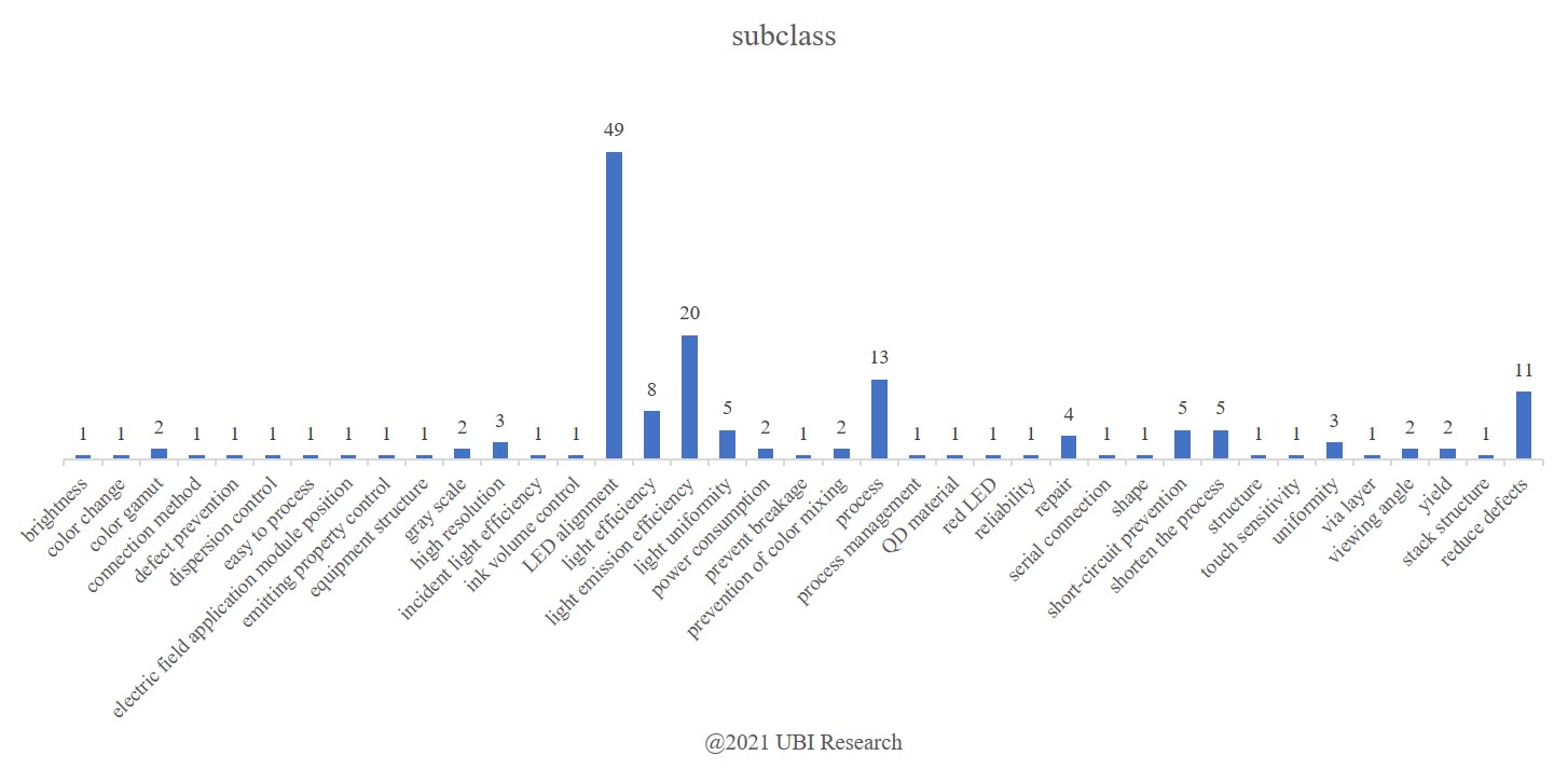


Professor Jang-Ung Park of UNIST Discusses Transparent Electrode’s Present and Future

During the International Advanced Materials & Application Technology Expo (November 25-27), Professor Jang-Ung Park of Ulsan National Institute of Science and Technology (UNIST) gave an in-depth lecture on transparent electrode’s new technology and research results under the presentation title of ‘Technology Trend and Development Direction of High Performance Transparent & Stretchable Electrodes Using Graphene and Ag Nanowire Complex’.


Transparent electrode is an electronic component with usually ≥80% transparency, and sheet tension of ≤500Ω/ㅁ of conductivity. This technology is widely used in electronics including LCD front electrode and OLED electrode in display, touchscreen, solar cell, and optoelectronic device.
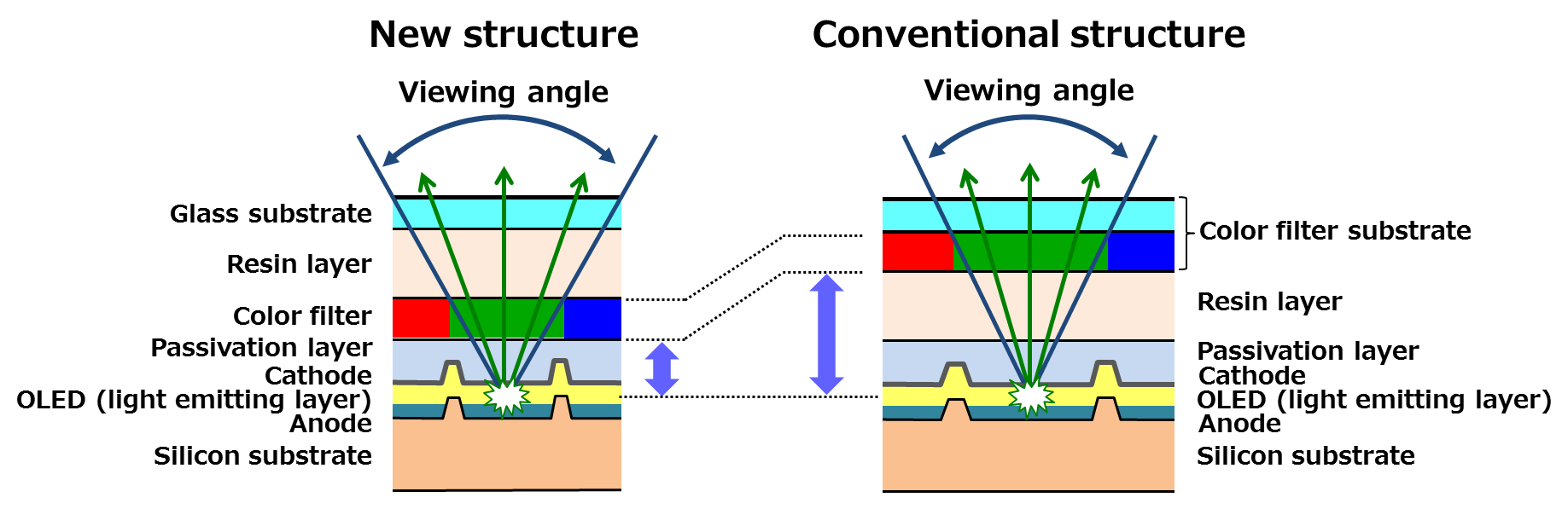
 

Park explained that the main market for transparent electrode is display and touchscreen, and announced that the transparent electrode market is to grow into US$4,800 million in 2020 from 2015’s US$ 3,400 million.


The electrode materials that is mainly being used at present is ITO (indium tin oxide) film produced through evaporation or sputtering. ITO’s merits include good conductivity from the low sheet tension and suitable for mass production. However, China is the main producer of the rare main material, indium, and has a drawback of high processing temperature. As such, research for indium replacement is continuing.


Graphene, CNT (carbon nano tube), Ag nanowire, and metal mesh are some of the materials that are in the spotlight as ITO replacement. However, Park emphasized that transparent electrodes that are being developed at present have difficulty in surpassing ITO in terms of electronical and optical properties. Instead, he explained that as the display shape changes, the replacement material can be used for displays where ITO cannot be applied.


At present, ITO is being used as the main electrode material for flat display. However, its weakness against mechanical stress and limitation in flexibility led to some views that flexible display application will be difficult. Regarding this Park explained that thickness of substrate is more important than ITO’s traits for display’s curvature radius and therefore if substrate becomes thinner, ITO can be applied even to foldable display as well as flexible. He added that although folding the display is acceptable, stretchable display is impossible as the properties are destroyed when pulled.
 

Park emphasized that in order for the wearable display market, including the smartwatch market, to grow, the comfort of the user is important. He reported as a human body does not conform to a specific curvature radius, to improve the user comfort, stretchable panel that can bend in diverse directions is a necessity. For this to be possible, transparent electrode that can replace ITO is required.


For example, watch shaped application can be replaced with stretchable display up to the strap part that wraps around the wrist. Glasses shaped application can have stretchable display for curved areas such as lenses. Also, within textiles industry, research into smart textiles through electronic circuit application is continuing.


As the transparent electrode that can replace ITO, Park suggested graphene and Ag nanowire complex. Ag nanowire reduces high sheet tension of graphene, and graphene prevents Ag nanowire’s oxidization, complementing each other. Park revealed that ≥90% transmittance and ≤30Ω/ㅁ was achieved through research. He emphasized as stretchability increased to 100%, it is suitable for stretchable display.
 

According to Park, transparent electrode can be applied to transparent stretchable sensor and transparent TFT as well as display. With confirmation of continued research regarding this issue, Park concluded his presentation.