ETRI Reveals Graphene Applied OLED Lighting

At R&D Korea 2015 (November 19-21), ETRI (Electronics and Telecommunications Research Institute) revealed OLED lighting and graphene related research results.


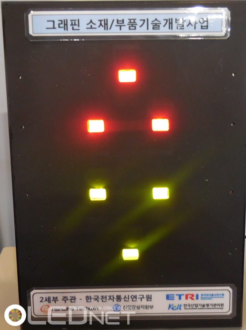
Since 2013, ETRI has been participating in ‘Graphene Applied OLED Device/Panel Technology Development’ project as a supervising organization. This project is a part of ‘Graphene Device/Component Commercialization Technology Business’, which is a Korean national project. This project’s ultimate aims include development of graphene electrode material with ≥15Ω sheet resistance, ≥90% transmittance, 3nm thickness, ≤5% sheet resistance uniformity, ≤5nm surface profile, and ≥5.5 generation area, graphene based protection layer that can be used for 5.5 generation 55inch OLED panel with ≤10-6 g/m2 WVTR, graphene anode OLED with ≥90% external quantum efficiency compared to ITO anode OLED, and diagonally 1300mm OLED panel prototype.


ETR1


In this exhibition, ETRI presented OLED lighting that used graphene as the electrode. ETRI’s Dr. Jeong-Ik Lee explained that recently interest in graphene electrode is increasing to replace ITO electrode and to apply graphene electrode, optical, electrical, and process issues have to be considered. When graphene is used as OLED electrode instead of ITO, thickness and refractive index change optically and electrically energy levels change, and these have to be considered when designing. He also emphasized that in terms of process, it has to be designed keeping in mind of before and after process of electrode procedure. Dr. Lee revealed that at present optical and electrical issues are solved while the process issues are in research stage, and they are planning to present the results of this research within this year.


Graphene, with its high resistivity, is known as next generation electrode material favorable to flexible and foldable. Dr. Lee pointed out that graphene has wider viewing angle than ITO when used as transparent electrode is another important advantage, and particularly as white light source’s spectrum cannot change according to the viewing angle, graphene is suitable for application.


Graphene is a key material with a wide arrange of applications, it is being developed in diverse areas such as OLED encapsulation as well as in electrode sector. The Ministry of Science, ICT and Future Planning of Korea estimated that domestic graphene market will record 19 billion KRW until 2025. Korea Evaluation Institute of Industrial Technology, the organization in charge of this national project, gave their target as developing 9 top technology through graphene and achieve 17 billion KRW sales. Regarding this, Dr. Lee emphasized compared to other countries, Korean investment in graphene is relatively low and that now is the time for the Korean corporations and government agencies to pay more attention higher value-added businesses.
[Expert Talk] Dr. Mauro Riva, SAES Group’s OLED/OLET Business Developer, on Encapsulation

Dr. Mauro Riva, SAES Group’s OLED/OLET business developer, discussed his views on OLED in general as well as SAES Group’s technology through his interview with the OLEDNET and presentation at the OLEDs World Summit (October 27-29) titled ‘The Encapsulation Question’.


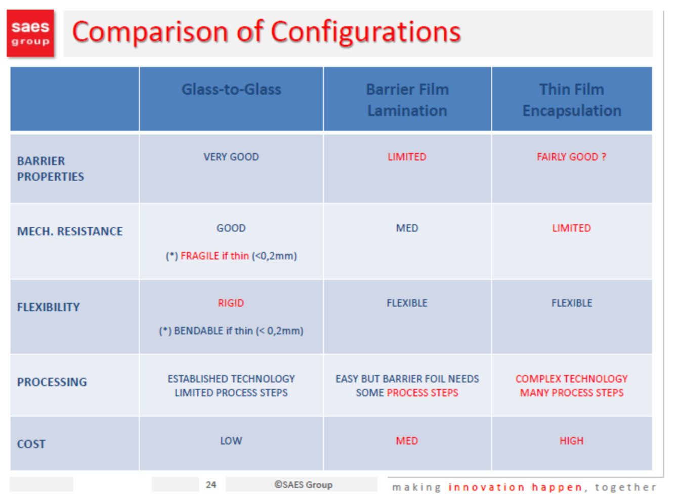
Encapsulation is required to prevent the oxidation of emitting and electrode materials by blocking moisture and oxygen. It also protects the device from mechanical and physical shocks. The basic configurations of encapsulation can be divided into 3: glass-to-glass, barrier film lamination, and thin film encapsulation methods. Glass-to-glass configuration is applied to rigid AMOLED for mass produced mobile, barrier film lamination and thin film encapsulation methods are used for flexible AMOLED, and barrier film lamination is used for large area AMOLED panel for TV.


Source: SAES Group, OLEDs World Summit 2015

Source: SAES Group, OLEDs World Summit 2015


According to Dr. Riva OLED encapsulation is still facing the same issues it had since the beginning: OLED materials’ extreme sensitivity to oxidizing agents and moisture in particular. He added that OLED materials can also be very sensitive to heat or radiations, generating many process constraints. Encapsulation technology is directly related to the lifetime of the OLED device and Dr. Riva raised several questions regarding the current issues surrounding the technology including the appropriate target lifetime, best definition of “lifetime”, and reliability of the “accelerated tests”. He emphasized that while much progress have been made, a “single optimal, universal solution” does not exist yet to meet various encapsulation requirements depending on OLED architecture, materials, environment, applications, etc. As such, encapsulation materials have to be specifically engineered to meet different types of OLED devices while having “exceptionally high barrier properties, and active fillers or getters, capable of absorbing water on a single molecule basis”. Thus, perfecting this technology is a very challenging task, and, according to Dr. Riva, something that requires in depth collaboration between advance encapsulation materials providers and OLED makers.


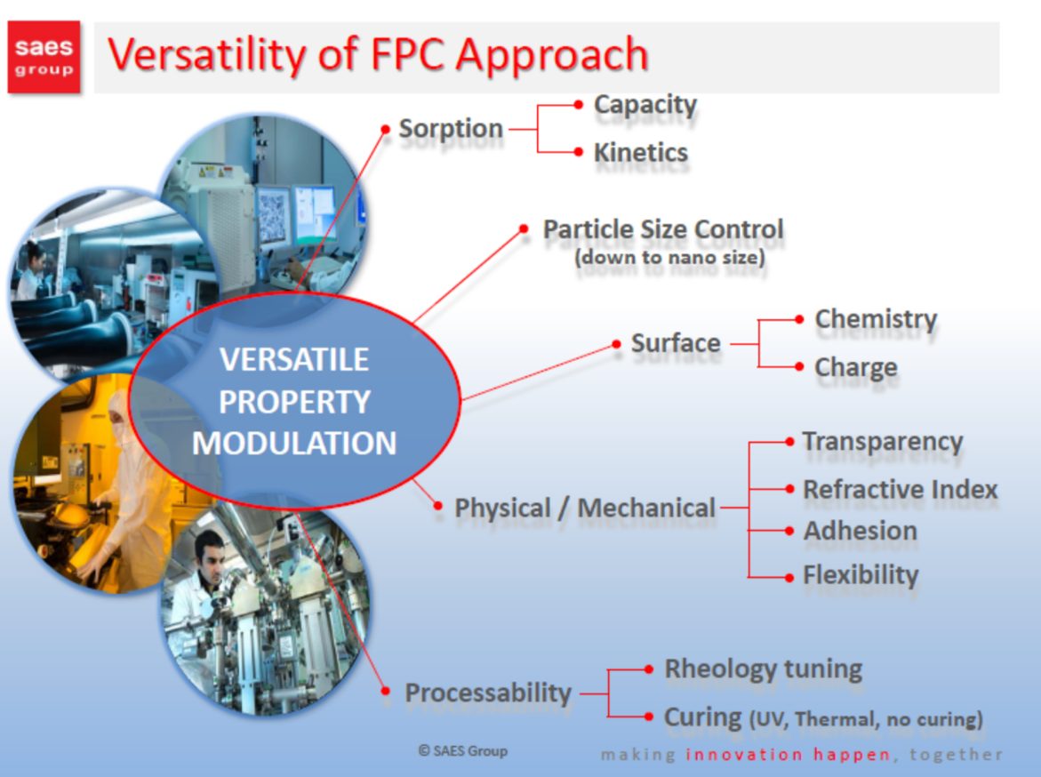
For their part in this technology progression, Dr. Riva reported that SAES Group provides a very large portfolio of active edge sealants, active transparent fillers, and dispensable getters. He explained that the portfolio is the results of deep know-how in functional polymer composites (FPC), “specially tailored to address customers’ specific OLED designs and processes”. Discussing the FPC during his talk in OLEDs World Summit, Dr. Riva emphasized the versatility of this approach.


Source: SAES Group, OLEDs World Summit 2015

Source: SAES Group, OLEDs World Summit 2015


Regarding application methods for SAES Group’s FPC products, Dr. Riva explained that they can be dispensed via screen printing, blading, syringe, ink-jetting, ODF (one drop filling), and even be employed in thin film encapsulation structures, to make them simpler and more reliable. Furthermore, Dr. Riva reported that while SAES Group considers syringe dispensing as one of the main methods for applying their FPC, “ink-jetting is also becoming more and more widespread, together with ODF, especially for active fillers”.


Dr. Riva believes the FPC could play an important role in making the encapsulation more effective, and that SAES Group can “leverage on its advanced materials expertise” and in-depth getter/purification knowledge, to “perfect FPC based encapsulation solutions for OLEDs”. 11% of SAES Group’s net sales is allocated to Research and Innovation every year with strong cooperation with universities and R&D centers. The company is collaborating with many companies in diverse areas of interest such as OLED lighting, manufacturing equipment, specialized food packaging, and gas barrier films. This proactive and collaborating approach will enable the SAES Group to play a key role in developing more marketable OLED devices.


Visionox Reveals 604PPI High Resolution AMOLED

On November 12, Visionox announced that they recently developed 604ppi (approximately 4.85inch) high resolution full color OLED panel through FMM (fine metal mask) using evaporation technology.


Visionox Z-Type(Source : OLED-info)

Visionox Z-Type(Source : OLED-info)


In 2014, Visionox developed 570ppi RGB AMOLED panel with newly developed pixel structure, Z-Type. This Z-Type arrangement had larger blue sub-pixel with green and red sub-pixels beside it. The new panel has resolution of 604ppi which is a 35ppi increase from the 2014 panel. With this new reveal, Visionox displayed their high resolution OLED technology improvement.


The 604ppi panel combined the self-developed pixel layout under proprietary intellectual property rights and co-developed Chinese FMM. The resolution is 2,560 × 1,440, manufactured using real RGB method and not pentile.


Chinese companies are developing their high resolution AMOLED panel technology at a fast pace. In August, EverDisplay presented 734ppi 6inch panel, and the technology difference with Korean panel companies is rapidly decreasing.


Visionox revealed that this OLED panel shows Visionox’s research development for high resolution OLED is continuing and aptly demonstrated the current results.


604 PPI High Resolution Display Panel (real RGB) (Source: Visionox)

604 PPI High Resolution Display Panel (real RGB) (Source: Visionox)

[IWFPE 2015] What Will Replace ITO?

2015 IWFPE (International Workshop on Flexible & Printable Electronics) was held at Le Win Hotel in Jeonju, South Korea (November 4-6). During the workshop, many OLED display related presentations commented on ITO’s replacement material.


Dr. Jennifer Colegrove, CEO of US research company Touch Display Research, discussed hot trends of 2015-2016. Dr. Colegrove included high resolution, transparent display, wearable device, and flexible display in the hot trends. Of these she pointed out ITO replacement material regarding touch panel. She mentioning metal mesh, silver nanowire, CNT, and graphene as materials that could replace ITO. Dr. Colegrove added that the material has to be flexible in order to be applicable to flexible display and needs to have high efficiency.


그래핀


Hanwha Techwin’s Dr. Seungmin Cho announced that graphene, which has higher uniformity compared to ITO, will be the material of future. With lower resistance than ITO, graphene shows good characteristics, but Dr. Cho explained that high cost and particles produced are issues that need to be solved. He also commented that China selected graphene related national projects and is striving to develop the technology.


Dr. Hyunkoo Lee of ETRI (Electronics and Telecommunications Research Institute) presented that the multi-layered graphene that ETRI, Sungkyunkwan University, and KAIST (Korea Advanced Institute of Science and Technology) co-developed will become the material that can replace ITO. He also introduced the results that as the transmittance is particularly high, it is suitable for transparent display, and compared to silver nanowire material in high resolution top emission structure, the display’s brightness is higher.


ITO replacement development is an issue for the future of display industry’s progress. It is estimated that research development on graphene as one of the ITO replacement electrodes will be actively carried out.


그래핀2

[IWFPE 2015] AUO’s Bendable AMOLED

During the IWFPE 2015 (November 4-6) held in Jeonju, South Korea, AUO gave a presentation on bendable AMOLED’s concept and technology first revealed in August.


AUO’s R&D manager Terence Lai reported that the bendable AMOELD can actualize new user interface through applying display’s bending characteristics and this can be the innovation that could change the existing touch interface.


AUO’s bendable AMOLED is 5inch with 295 PPI using the LTPS TFT and hybrid encapsulation with top emission structure. It has 02.mm thickness and through bending sensor of file type, it can process diverse functions by detecting different bending directions.


Current flexible AMOLED trend is moving from curved to foldable, jumping past bendable. Key panel companies and research laboratories are focusing on developing foldable.


It is anticipated that the AUO’s bendable AMOLED panel will provide new direction for the flexible AMOLED development that is heading toward foldable. Development of applications suitable to bendable and functions that utilizes bending characteristics are expected to be key issues.


AUO's 5" Bendable AMOLED Prototype

AUO’s 5″ Bendable AMOLED Prototype

Attention Focused on Silver Nanowire as Key Material for Display

At IPEC 2015 (International Printed Electronic Conference), held on September 1, Professor Sang-Ho Kim of Kongju National University announced that silver nanowire technology is in initial stages of commercialization and will become display market’s key material.


Kim reported that when the bending radius of flexible display is reduced, 2 key issues occur with silver nanowire used as TSP (touch screen panel) material. First, the wiring that are crossed when bending is loosened as can be seen in figure 1. Due to this effect the bending stability decreases.

Fig. 1, Source: Professor Sang-Ho Kim, IPEC 2015

Fig. 1, Source: Professor Sang-Ho Kim, IPEC 2015


Kim explained that this effect can be solved by welding the two wires as shown in figure 2 using thermal annealing technology, laser process, and IPL photo-sintering technology.


Fig 2, Source: Professor Sang-Ho Kim, IPEC 2015

Fig 2, Source: Professor Sang-Ho Kim, IPEC 2015


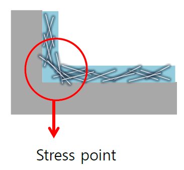
Another issue is a decrease in contact stability between nanowires at stress points when bending radius is reduced as shown in figure 3.


Fig 3, Source: Professor Sang-Ho Kim, IPEC 2015

Fig 3, Source: Professor Sang-Ho Kim, IPEC 2015


During the presentation, Kim explained that this can be solved through undercoating process. This process involves mixing 2 polymers with different Tg (glass-transition temperature) and layering it as in figure 4, and placing TSP on top.


Fig 4, Source: Professor Sang-Ho Kim, IPEC 2015

Fig 4, Source: Professor Sang-Ho Kim, IPEC 2015


Silver nanowire has benefit of being more flexible and less resistant compared to transparent electrode material, ITO. As such, it was spotlighted as TSP material most suitable for flexible OLED. Nonetheless, silver nanowire has been considered to fall behind ITO in panel mass production unit cost in display market.


However, haze effect which happens when sunlight is reflected off the silver nanowire TSP has been solved recently, and new touch technology that requires improved TSP functions, such as post-touch technology, has been developed. Accordingly, products that use silver nanowire are increasing despite the unit cost difference.


Kim reported that as TSP sheet resistance can be reduced through undercoating and welding technology and greatly increase bending stability, it is estimated that silver nanowire’s marketability will grow for flexible display.


[IMID 2015] UDC Develops OLED Patterning Technology with Less Masks

At present, FMM (Fine Metal Mask) is considered the main method for large area RGB OLED panel production. However, due to shadow effect, mask total pitch fluctuations, and mask slit tolerance issues, there is a yield limitation to this technology. This limitation increases as the resolution becomes higher; minimizing the number of FMM during the OLED panel production has been a key issue in RGB OLED production.


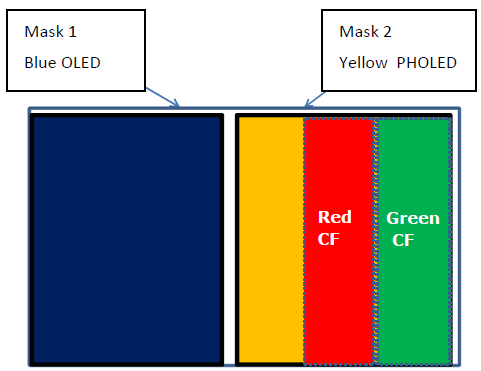
In SID 2014, through a paper titled “Novel Two Mask AMOLED Display Architecture”, UDC revealed a technology that can reduce the number of masks used in RGB-FMM method to 2 from previous 3.


Source : UDC, SID 2014

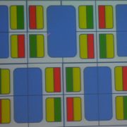
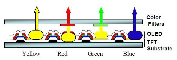
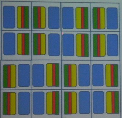
As shown above, this technology coats yellow and blue subpixels using 1 mask each. Following this process, green and red color filters are applied above the subpixels. Pixels are formed as illustrated below.


Source : UDC, SID 2014

UDC explained that this technology improves lifetime of the display overall and reduces energy consumption as blue voltage can be lowered. Additionally, tact time can be reduced through this technology, and increase the yield.


In IMID 2015, UDC presented research of the same title. However, the content of the presentation unveiled more developed research compared to 2014. First of all, in 2014, UDC announced that the panel’s lifetime could be improved by 2 times compared to the RGB method. In IMID 2015, UDC’s announcement changed the figure to 3.3 times increased lifetime.


UDC also revealed that the technology can be actualized through printing method, and has the advantage of being able to print 2 rows of pixels at once. UDC announced that this is most suitable when OVJP (Organic Vapor Jet Printing) applies the printing method.


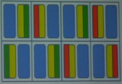
A new technology called SPR (Sub-Pixel Rendering) was also announced by UDC in this paper. The 2014 SID paper included a method that did not uses SPR. As shown below in figure 1, 4 subpixels of RGY and B are used per pixel.


[Fig. 1], Source: UDC, IMID 2015

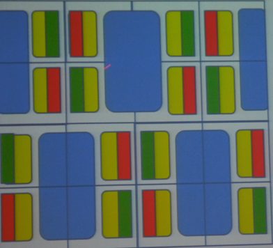
During IMID 2015, UDC presented APR technology applied pixel structure. Figure 2 shows 3 subpixels per pixel.


[Fig. 2], Source: UDC, IMID 2015

In this case, as the pixels can be arranged as shown in figure 3, smaller number of subpixels can be used.


[Fig. 3], Source: UDC, IMID 2015

UDC announced that because APR technology allows the number of subpixels per pixel to be reduced to 3 or less, the number of data lines and TFT per pixel can also be reduced together.


UDC explained that this technology can be applied regardless of the display area or resolution, and will be able to be applied to different types of panels.


HUD and HMD Meet Virtual Reality and Soar

At SID 2015 Review Workshop held in Konkuk University on July 31, Inha University’s Associate Professor Jae-Hyeung Park announced that interest in HUD (head-up display) and HMD (head-mounted display) increased at SID 2015.


HUD signifies technology that provides diverse information for the driver beyond the role of a front glass that simply allows the outside to be viewed and provides protection. Through HUD, drivers can grasp vehicular and destination information without having to take eyes off the road. At this juncture, AR (augmented reality) HUD is more than a simple display as it recognize the user’s movements and applies it to the display.


In SID 2015 paper, Japan’s Ricoh termed the device that self-intervenes in the vehicular operation as ADAS (Advanced Driving Assistance System) and announced that the information from the device applied to HUD will be able to help the user’s recognition and decision making. It was also added that improved AR can be realized when the contrast range is increased to be equal to reality and reiterated and the distance from the virtual image is 5m.


HMD, as a head-mounted device, provides differentiated feelings of immersion compared to other displays. Due to the increased realism from the wide viewing angle, HMD was widely used as an entertainment display, but with the recent increased interest in AR, it is receiving much spotlight as an AR display device.


At SID 2015, the West Saxon University of Applied Sciences of Zwickau revealed an HMD device that actualizes AR naturally by changing the distance where image is shown according to the use by adjusting the focal distance. Zhejiang University’s college of Optical Science and Engineering used method of showing hologram to each user’s eyes using the light field concept that realizes the light strength to all directions from all points in 3D and produced improved AR.


Park explained that with SID 2015 as a starting point, the AR related HMD and HUD interest and research will increases greatly and that the trend will continue in future.


Samsung Electronics released HMD device Samsung Gear VR that can be used by plugging in to Galaxy S6 or Galaxy S6 Edge. Oculus VR and Sony Computer Entertainment each revealed OLED applied VR headset Oculus Rift and Project Morpheus, and scheduled release regular product in Q1 and H1 of 2016 respectively. Korea’s HLB released AproVIEW S2 which used virtual image distance actualization method, a first for HUD.


Inha University’s Associate Professor Jae-Hyeung Park at SID 2015 Review Workshop

Encapsulation Technology That Can Greatly Increase OLED Lifetime Unveiled

On July 29, at Chungcheong Display Forum held in Hoseo University in South Korea, an encapsulation technology that can greatly increase OLED lifetime was revealed.


Encapsulation technology prevents permeation of oxygen and moisture from affecting OLED panel’s performance and increases lifetime. As it is also the last process that decides OLED panel yield, OLED panel manufacturing companies are focused on finding the most optimal encapsulation technology.


The flexible OLED panel that is currently being mass produced uses hybrid structure of encapsulation where gas barrier cover plate is applied to the organic and inorganic stacks of passivation.


During this process, because cover plate with gas barrier characteristics is the key factor in deciding encapsulation performance the materials and technology are very important. The level of encapsulation that OLED panel requires is approximately 10-6g/m2day. The unit signifies the amount of permeation for 1m2 area a day. This amount is same as 1 drop of water in an area size of 6 World Cup stadiums.


Generally sputtering technology is used to form gas barrier layer. Sputtering technology is an evaporation technique where ions of the target material is coated to the substrate as noble gas, ionized via high voltage, collides against coating material.


This type of sputtering technology creates particles and defects during process. As such, in order to be applied to OLED, multilayer is required leading to a decrease in productivity and increase in production cost.


However, at the Chungcheong Display Forum, Professor MunPyo Hong of Korea University, revealed that defect that occurs during the existing sputtering process can be reduced by stabilizing target layer through installing reflector which induces neutral beam to be released.


According to Hong, this technology is sufficient to achieve the OLED level encapsulation standard of 10-6g/m2day even using a single layer. He revealed that this technology will be able to reduce the production cost and increase the productivity.


(a) Device Immediately After Production (b) Device with Insufficient Encapsulation with Insufficient Encapsulation (dark spot and pixel shrinkage occurs after certain amount of time) Source: UBI Research

A Place Where the Latest OLED Technology Trend Can Be Seen In One Glance UBI Research Hosts 2015 OLED Key Technology Seminar

A seminar where latest technology of next generation display, OLED (Organic Light Emitting Diode), can be easily understood will take place. UBI Research, a research company specializing in OLED (http://www.ubiresearch.co.kr, president: Dr. Choong Hoon Yii), revealed that it will hold 2015 OLED Key Technology Seminar in COEX (Samseong-dong, Gangnam-gu, Seoul, South Korea) on 27 Aug.

This seminar will discuss latest issues in OLED industry such as processes in flexible OLED, encapsulation, oxide-TFT, blue phosphorous emitting material, and solution process, and focus on technology development and its future.

Encapsulation, which decides OLED panel’s final yield and lifetime, is an important process that determines exterior design in flexible OLED and large size OLED panel. It is also sensitive to light characteristics in surface light structure. At the 2015 OLED Key Technology Seminar, Dr. Choong Hoon Yi (president of UBI Research) is scheduled to introduce, through process and material analysis, essential technology needed for OLED panel to continue its growth and encapsulation technology trends.

At this seminar, Dr. Nam Sung Cho of ETRI (Electronics and Telecommunications Research Institute) will give a presentation on display technology that utilizes white OLED technology that is receiving much interest by Korean display market. He will detail white OLED technology’s present and future from lighting to large size TV.

Professor Sung Kyu Park of Chung-Ang University, will introduce oxide material that is in spotlight as display and next generation wearable device. He will also talk about internationally much discussed related technology trends and future progress.

Further presentation topics by OLED top experts include:

– AMOLED panel technology trends analysis (Hyun Jun Jang, senior researcher of UBI Research)

– Oxide-TFT technology status (Professor Ga-Won Lee, Chungnam National University)

– Solution process and vacuum evaporation OLED material’s status and forecast (Professor Sung-Ho Jin, Pusan National University)

– High efficiency blue phosphorous emitting material development trend (Professor Jun Yeob Lee, Sungkyunkwan University)

– Flexible OLED technology trend

UBI Research holds OLED Key Technology Seminars every year from 2011 and provides place for networking and sharing of information. Seminar registration can be completed through UBI Research website (www.ubiresearch.co.kr).

프로그램2

OLED 8K TV, When Would It Be Possible?

The current TV market trends are curved design, large area, and high resolution. LCD and OLED, competing to lead the next generation display market, have both released curved large size premium TV of 55 inch screen or larger. In terms of resolution, UHD grade products are being released following FHD, and displays with higher resolution are being required.


Looking at Korea and Japan’s contents roadmap, UHD resolution OLED TV development is essential as Japan is aiming to test 8K contents broadcasting in 2016, and Korea in 2018. Korea began test broadcasting UHD from 2013, and is aiming for regular application in 2016 for satellite/cable channels and 2018 for broadcast channels. Considering active release of UHD TV occurred in 2014, 8K TV’s market release is estimated to be in 2019-2020. It is analyzed that approximately 3 years are left to prepare for 8K TV mass production.


At present 8K LCD TV have been revealed by key panel companies through various exhibitions, and its mass production is set for 2016-2017. However, only up to 4K OLED TV have been unveiled, falling behind LCD in terms of resolution.


The keys to 8K OLED TV actualization are pixel size reduction and aperture ratio achievement. LCD uses 1 transistor and capacitor per pixel whereas OLED requires 2 or more transistors and 1 capacitor per pixel. This leads to OLED’s difficulty in acquiring adequate aperture ratio and reducing pixel size compared to LCD. The key solutions are developments of top emission structure of OLED panel for TV, instead of bottom emission that produces light through TFT, and emitting materials that can generate sufficient light efficacy from bottom emission produced aperture ratio.


OLED demonstrated its strength as display by achieving what LCD took more than 10 years in 2-3 years. Considering this, although approximately only 3 years are left to mass produce 8K display, it is anticipated that OLED is capable of catching up to LCD’s resolution.

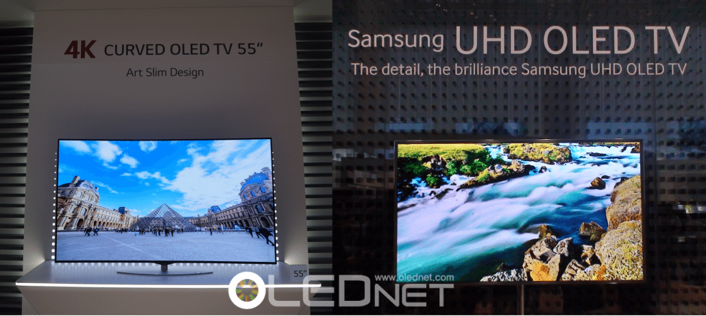
4K OLED TV by LG Display and Samsung Display

New Solution for Next Generation OLED Lighting

Professor Lee Taek Seung of Chungnam National University

Professor Lee Taek Seung of Chungnam National University


Professor Taek Seung Lee and Jongho Kim (Chungnam National University’s Department of Advanced Organic Materials and Textile System Engineering), and Professor Jin Sung-Ho and Park Juhyeon (Pusan National University’s Graduate Department of Chemical Materials, and Institute for Plastic Information and Energy Materials) authored a paper titled ‘Synthesis of conjugated, hyperbranched copolymers for tunable multicolor emissions in light-emitting diodes’. For 2015 June issue, Polymer Chemistry, published by the Royal Society of Chemistry, selected it as its back cover.


The paper discusses research of polymer material applied to solution process and explains that through polymer structure in the form of hyperbranched red, green, and blue monomers, diverse colors, including white, can be actualized depending on the amount of each monomer. Existing OLED lighting used R/G/B or YG/B stacking structure to produce white OLED, complicating the process. Although a method of producing white by combining R/G/B together is being developed, energy displacement between R/G/B can cause unwanted colors. However, if the R/G/B monomers can be introduced to polymer structure as hyperbranched forms as the paper suggests, the energy displacement can be minimized when the polymer solidifies which makes it easier for the colors to be realized.


Professor Lee revealed that hyperbranched polymer materials were used in the research and that as white can be produced from just one polymer material, simple process can be used for the production.


The patent for this technology has been applied (application number 10-2012-0091350) in Korea. It is anticipated that this will become a key technology for reducing the next generation OLED lighting production cost.


원리

[SID 2015] AUO’s New RGBY Pixel Structure, Can It Be an Answer for Low-Powered OLED?

Display consumes most power out of smartphone battery usage. This means that low-powered display is most important in lengthening the smartphone’s usage time.


AMOLED panel is a self-illuminating device driven by each RGB subpixels, and theoretically power consumption should be much lower than LCD’s which requires BLU (back light unit) to be constantly lit. However, as OLED materials’ performance, particularly blue, is not sufficient the power consumption falls short of expectation.


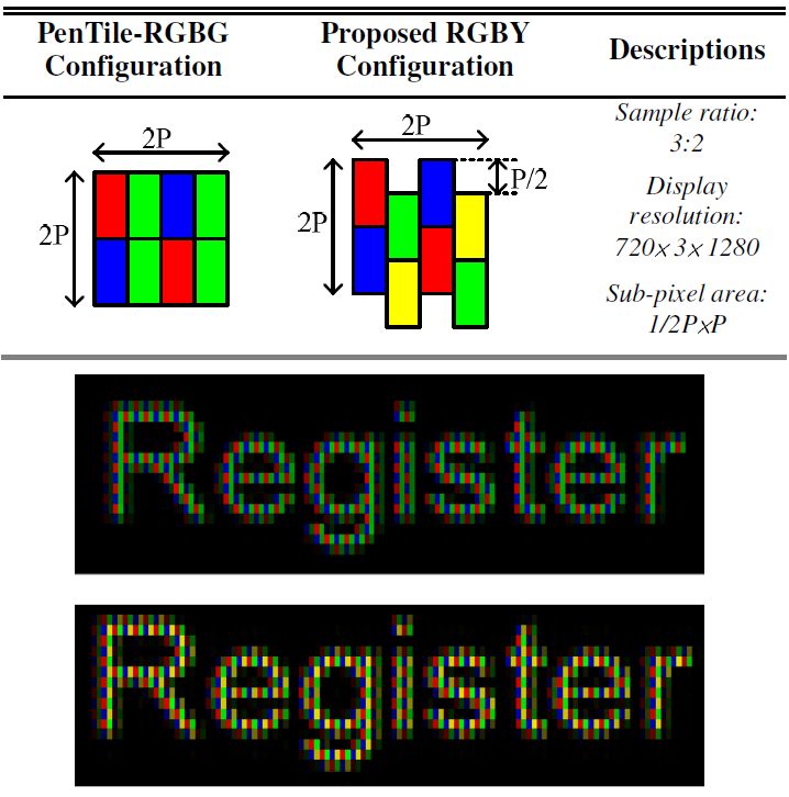
In SID 2015, AUO gave a speech on new RGBY pixel structure attempting to solve the power consumption issue. AUO applied PSA (power saving algorithm) and SPR (sub pixel rendering) of RGBY method, not RGBG structure’s pentile method of existing FMM RGB mechanism, and reported that this showed higher definition and lower power consumption compared to the pentile method RGB applied for high resolution. Particularly it was shown that it can be a key technology for low-powered AMOLED panel through HD 4.65inch (317ppi) panel demo; the power consumption of yellow sub pixel (efficiency 80-120 cd/A) was reduced by 16-20% in comparison to existing RGB method.


Dr. Meng-Ting Lee of AUO told the audience yellow sub pixel application improves high resolution, high definition, low power consumption, and panel’s lifetime simultaneously and that AUO’s RGBY SPR and PSA technology can become key technology for AMOLED panel for mobile device.


AUO’s RGBY Pixel Structure, SID 2015

AUO’s RGBY Pixel Structure, SID 2015


Comparison of Power Consumption Between RGB and RGBY

Comparison of Power Consumption Between RGB and RGBY

Seoul National University’s Research Team Lead by Professor Changhee Lee Succeed in Developing High Output QLED Emitting True Ultraviolet Light

South Korean research team lead by Professor Changhee Lee in Seoul University succeeded in making first quantum dots that emit ultraviolet light and used them to produce a flexible, light-emitting diode.

UV light is usually produced by mercury lamps or LEDs made from inorganic materials such as gallium nitride (GaN). However, mercury lamps tend to emit a wide range of visible wavelengths as well as UV, and high-performance gallium nitride LEDs are expensive to make. According to Professor Lee, quantum dots are an attractive alternative which can be made using potentially less expensive solution-based processes.

Quantum dots, made out of a semiconductor material, emits different wavelengths depending on the size and shapes. The smaller the crystal, the shorter the wavelength of the light it emits. The Professor Lee’s team is the first in succeeding in making quantum dots that emit wavelengths shorter than about 400 nm, the high end of the UV spectrum.

In order to produce UV nanocrystals, the team had to figure out how to make quantum dots with light-emitting cores smaller than 3 nm in diameter. To make these, the team utilized cadmium zinc sulfide, which emits high-frequency light, zinc sulfide shell. The quantum dots produced through this method emit true UV radiation at about 377 nm. Professor Lee explained that they “can go to much shorter wavelengths than people generally expected from quantum dots”.

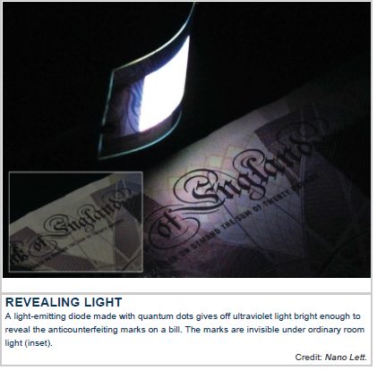
The research group then made a flexible LED with the quantum dots, using a design for a high-efficiency device they developed in 2012. Professor Lee’s team showed that the UV LED could illuminate an anticounterfeiting mark in a bill of paper currency. Franky So, a materials scientist at the University of Florida, says making a device out of the quantum dots that shines brightly enough to reveal the currency mark is a remarkable accomplishment. If their lifetimes can be improved, these potentially low-cost UV LEDs could find uses in counterfeit currency detection, water sterilization, and industrial applications.

The research team headed by Professor Lee includes Seoul National University, Professor Seonghoon Lee and Professor Koonheon Char, and Dong-a University’s Professor Jeonghun Kwak. The research was published in Nano Letters (Nano Lett. 2015, DOI: 10.1021/acs.nanolett.5b00392), a monthly peer-reviewed scientific journal, and reported on Chemistry & Engineering (27 May), published by the American Chemical Society.11

Why Hybrid Encapsulation?

The latest trends in the display market can be represented with the keywords such as flexible, large panel and high resolution. And companies are releasing the products applying a flexible AMOLED panel like Galaxy Note Edge, Galaxy Gear S, and G Watch R and high-resolution products applying a large area panel such as UHD curved 65- and 77- inch in the AMOLED market. For Flexible AMOLED panel, foldable and rollable features are required whereas the resolution over UHD level and the brightness at least 500nit are required for a large area AMOLED panel.


There still are many issues to be resolved to mass-produce a flexible AMOLED panel and a large area AMOLED panel with the resolution above UHD level. Especially the encapsulation is a technology deemed to transform as the OLED manufacturing technology changes and it is a very critical area for it is the last process determining the panel yield rate.

Encapsulation is essential process to prevent emitting and electrode materials from being oxidized as it blocks moisture and oxygen flowing in from the outside of OLED element, and protects elements from mechanical and physical impacts from outside.

According to the “OLED Encapsulation Report” issued by the UBI Research on the 5th, the key encapsulation technology applicable for every application is expected to be the hybrid encapsulation.

The Hybrid Encapsulation structured with a thin-film passivation, a cover plate with a gas barrier property, and polymer to adhere a thin-film passivation and cover plate in two applications ? the ‘Dam & Fill’ uses polymer in liquid form while the ‘Film Laminating’ uses it as processed in film form.

14210212719

The frit glass method which is employed in the rigid AMOLED for a mobile device currently on sale is a perfect encapsulation method but it is hard to be applied to a large panel and flexible AMOLED. The TFE (Thin Film Encapsulation) technology which is applied to some flexible AMOLED is also inapplicable for a large panel due to the complicated process of forming a multilayer thin film, the occurrence of particle, and the problem of film uniformity.


However, the hybrid encapsulation is valid for both a large panel and flexible OLEDs with the advantage that the number of process is less than that of TFE. UBI research analyzed that the hybrid encapsulation using a transparent gas barrier can be applied to a rigid AMOLED panel for a mobile device for the benefits of preventing breaks and reducing thickness.


As the hybrid encapsulation is applied in a large area OLED and flexible OLED panels which is to be the core of future OLED industry, UBI Research prospected the main material market for hybrid encapsulation to form US$600 billion in 2015 and to show CAGR of 74% between 2015-2020. The primary materials applied in the hybrid encapsulation are organic materials, metal foil and transparent gas barrier.

SolMateS developed ITO deposition technology without damage

The Dutch deposition equipment specialized company SolMateS unveiled the new OLED deposition process.

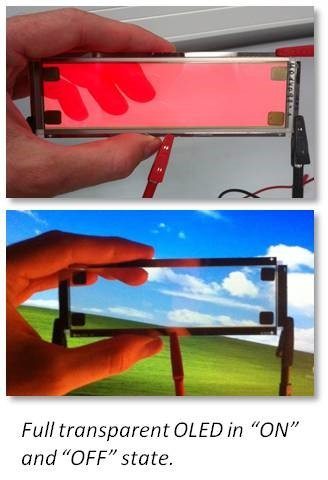
The newly developed deposition process by the SolMateS is a full transparent OLED called ‘soft-landing’ based on SolMateS’ pulsed laser deposition (PLD), which already obtained the patent. According to the SolMateS, the existing deposition technology like sputtering may cause damage to organic layers whereas the ‘soft-landing’ method enables to put an ITO thin layer on top of the OLED without damaging as it is proceeded in an even process temperature.

And recent test result shows not much difference in their functions between the OLED of 80% transparency and aluminum electrode OLED of no transparency. The ITO was deposited in the speed of sputter and PLD tool of 200mm is possible.

Arjen Janssens, the CEO of SolMateS mentioned that ‘PLD technology can be applied to various OLED applications using multiple transparency such as transparent lighting, display, smart window or top emitting OLED display, and it will be of great help for highly efficient organic solar cells.’

Established in 2006 in the Netherlands, the SolMateS is the deposition equipment supplier based on the laser deposition.

141111_SolMateS

Source – SolMateS

reporter@olednet.co.kr

LGD, Plastic OLED Technology Announcement

LG Display (LGD) is promoting actively as unveiling the plastic OLED technology applied to its own G Watch R.

It is published under the title ‘The New Advancement in Display technology: LG Display’s Plastic OLED’ on the LGD’s U.S Newsroom (http://lgdnewsroom.com/) and the contents are as follows.


The New Advancement in Display technology: LG Display’s Plastic OLED

What is Plastic OLED?

Plastic OLED is an OLED that is made out of plastic substrate. There are 4 very special key technologies applied to this OLED.

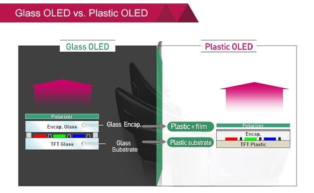
1) Plastic, not glass

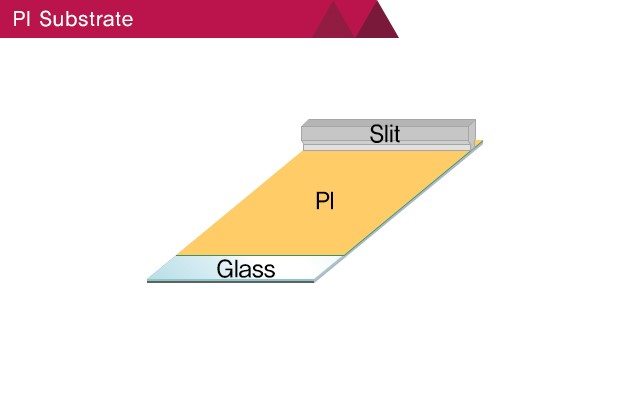
LG Display has shattered the common belief that plastic cannot stand high temperatures, and developed plastic substrate (PI or polyimide) that remains stable under high temperatures and has chemical stability. Moreover, due to the development of the coating process of large format PI, it has become possible to manufacture PI film, which has enabled the plastic curving technology and the technology to eliminate unnecessary bubbles and foreign substances.

141110_LGD,POLED

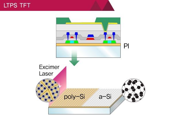
2) LTPS(Low Temperature Poly Silicon) TFT(Thin Film Transistor) technology

One of POLED’s important features is that it can have thin bezel, since the fast electron mobility technology made the integration of different parts to be possible.

141110_LGD,POLED1

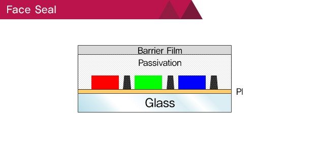
3) Flexible Encapsulation Technology to protect OLED elements

With the technology to manufacture inorganic film that prevents water and organic film that prevents alien substances, plastic OLED guarantees the stability of OLED elements.

141110_LGD,POLED2

4) Elimination of Carrier Glass using laser, and adhesionof Back Plate Film

The display surface is relatively clean and neat, as it prevents foreign substance from permeating the surface, by using Laser Source Uniformity technology, alien substance/crack prevention process technology, and flat-panel Back Plate Film and Film Lamination technology.


Why Plastic OLED?

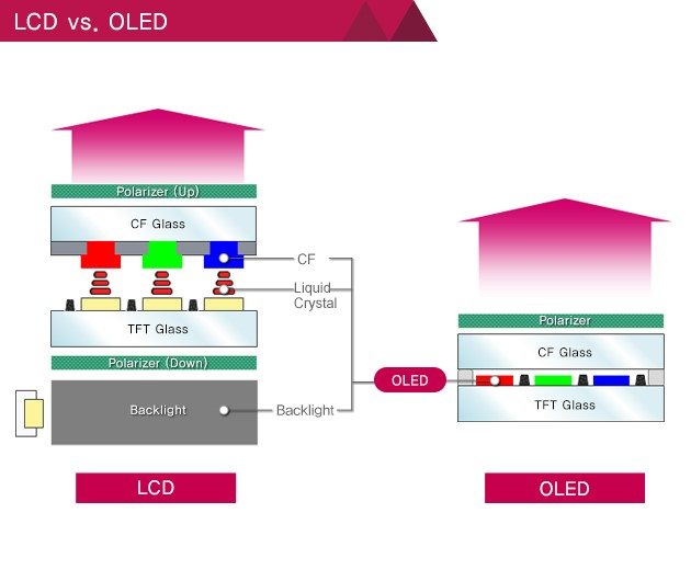
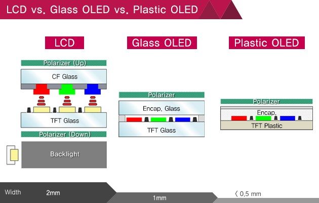
1)Compared to currently existing displays, Plastic OLED has simpler structure. As it can be seen from the diagram below, LCD is composed of many layers of boards, while OLED’s structure is very simple.

141110_LGD,POLED3

2)While glass displays are prone to breakage, Plastic OLED, which is film based, is flexible to be curved to a certain angle, and it does not break easily.

141110_LGD,POLED4

3)Compared to LCD and glass OLED displays, Plastic OLED is thinner and lighter.

141110_LGD,POLED5

The future of Plastic OLED

As Plastic OLED can be applied to curved displays that are bent to a certain curvature, it can be used in various ways, including electronic goods, such as mobile phones, monitors, and TV, as well as cars, wearable devices, and items for interior design.

Other than its design, Plastic OLED is valuable in terms of portability and durability as well. Hence, it seems that Plastic OLED will play an important role in people’s everyday lives in the future.

141110_LGD,POLED6.jpg

The Plastic OLED’s potential is very promising. LG Display is devoting its energy and resources to respond quickly to fast growing market and consumers’ needs in order to develop Plastic OLED to become the key OLED application technology in the future.


Source – LG Display Newsroom

reporter@olednet.co.kr

Solution Processing OLED Era is coming

At the International Workshop on Flexible & Printable Electronics, IWFPE held in Jeonju, Konica-Minolta and DuPont presented diverse technologies that converts the OLED production process which requires a glass substrate into the technology of using a flexible substrate and printing technology.

Konica-Minolta is under development of the OLED panel for lighting and the production of a flexible OLED panel as a printing technology of R2R method for the first time in the world is imminent. Based on the camera film production technology, Konica-Minolta has a wide range of light-emitting materials technology and also the R2R technology at the same time, getting attention as a front-runner to open a new era of flexible electronics.

DuPont is the pioneer of the solution processed OLED display business as well. Equipped with the nozzle printing method which is its own printing technology, it continued to research and develop for many years with Samsung Display. The most critical benefit of the solution OLED is that it is the only technology to manufacture a large area OLED panel over 55-inch with RGB method at a large equipment bigger than the Gen8. DuPont completed the technological development of containment creation, ink deposition, and ink drying which are the essential technologies for the production of the solution OLED panel and is accelerating the commercialization. DuPont prospects that the solution OLED panel market will be open within three years at the latest.

reporter@olednet.co.kr

Development of the high efficiency solution processed fluorescent organic light-emitting device

141107_단국대 이준엽 교수

Korean researchers have developed the highly efficient florescent organic light-emitting device which enables to enhance the efficiency more than three times and is receiving much attention as the next generation display.

This research by the Prof. Jun Yeob Lee, the Ph.D. candidate/researcher Yong Joo Cho (the 1st author) and the Prof. Kyoung Soo Yook from the Department of Polymer Science and Engineering at Dankook University was supported by the Mid-career Researcher Program funded by the Ministry of Science, ICT and Future Planning and the National Research Foundation of Korea as well as the General Researcher Program funded by the Minister of Education and the National Research Foundation of Korea, and the research results were published on the Advanced Materials which is the international journal covering  materials science on the 15th October. (Paper Title: High Efficiency in a Solution-Processed Thermally Activated Delayed-Fluorescence Device Using a Delayed-Fluorescence Emitting Material with Improved Solubility)

Using the solution processing, it is expected to ease and simplify the process of producing the organic light-emitting device as the large area compared to the existing vacuum deposition plating.

However the problem is that when a device is produced through the solution processing using the existing fluorescent emitting material, the efficiency (external quantum efficiency) is only 5%. This is much less than the 20% which is the efficiency when produced by the vacuum deposition plating process.

The research team developed the high efficiency fluorescent organic light-emitting device, improved three times more than the previous fluorescent device for the solution processing. Compared to the existing structure, a solubility was increased by introducing the alkyl group as a substituent. Furthermore, the Donor-Acceptor Structure was employed to realize high efficiency by inducing delayed fluorescence phenomenon.

It is anticipated to advance the commercialization of a large scale organic light-emitting device for the enlargement of a future display.

The decrease of efficiency issue was resolved by making the surface film coating of a device smooth through the development of a new fluorescent light-emitting material which is soluble in organic solvents.

And introducing the strong Donor – Acceptor structure, it was possible to improve the efficiency as drawing delayed fluorescence phenomenon. The Donor – Acceptor structure refers to a monomer composed of an entity that donates electrons to another compound and that accepts electrons transferred from another compound.

Professor Lee revealed that “The following research will be continued to commercialize the solution processed fluorescent organic light-emitting device by developing a new material to improve not only the efficiency but also the lifespan of a device and a device structure appropriate for a solution processing.”

reporter@olednet.co.kr

What is the optimal encapsulation technology for the Flexible AMOLED?

Currently mass-producing flexible AMOLED panels are taking PI substrate, backplane, and RGB deposition method, and the existing encapsulation technologies for A2 line of Samsung Display is TFE (thin film encapsulation) and hybrid encapsulation for LG Display.

But for the flexible AMOLED exclusive A3 line which is newly invested by the Samsung Display, advanced the orders not in the TFE but in the hybrid encapsulation method which is laminating the film after resin coating process on the passivation structure of inorganic layer and organic layer, similar to the method that the LG Display takes.

The reason for the change of encapsulation technology at the A3 of Samsung Display was analyzed in the “2014 Flexible OLED Report” issued by the UBI Research including the latest trends and issues such as the flexible AMOLED related issues and processes, market forecast of the flexible AMOLED panel and flexible OLED lighting, flexible AMOLED technologies comparison of Samsung Display and LG Display, etc.

According to this report, the flexible AMOLED panel market is forecasted to show a compound annual growth rate of about 60% through to 2020, reaching $ 17,600 million where the primary applications are expected to be for the flexible AMOLED panel of tablet pc.

140926_Flexible AMOLED용 encapsulation, 최적의 기술은

<Flexible AMOLED panel Market Forecast>

reporter@olednet.co.kr

OLED TV cost saving, the alternative is co-planar structure

Current AMOLED panel market is mainly led by either Samsung Display or LG Display, mass producing the LTPS backplane for mobiles and Oxide backplane for TVs.


Though the AMOLED panel market for mobiles has established stable position in the business beyond LCD panel market, the market for TV is having difficulties in settling for its high price compared to the LCD/LED TV, requiring pressing technological development to lower the cost.


As a counterplan for this, the LG Display received a considerable attention at the SID 2014 by exhibiting 65-inch curved UHD OLED TV applying not the existing etch stopper layer (ESL) structure but the co-planar structure.


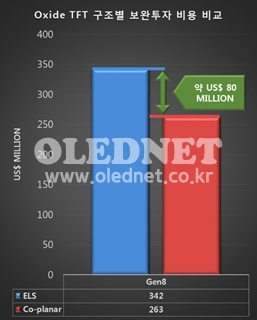
According to the “2014 AMOLED Backplane Technical Report” published by the UBI Research, it was analyzed that there is a difference in the investment expenses by about $ 80 million when making the additional investment in oxide TFT AMOLED line of co-planar for a-Si LCD line against the supplementary investment in oxide TFT AMOLED for LCD line. (For Gen 8) It was also suggested that the co-planar structure is appropriate for the oxide TFT structure which can make the best use of the backplane and color filter equipment of the previous a-Si LCD line as the mask can be used under 6 layers.


In addition, the core issue of the AMOLED industry which is a technological concern over the flexible LTPS applied to the flexible display was examined along with the latest technology trend analysis of LTPS, oxide, and organic TFT in the “2014 AMOLED Backplane Technical Report”.

003

reporter@olednet.co.kr

KITECH, Developed the world’s first refining technology for organic light-emitting material using ILs for OLED TV

Dr. Taewon Kim’s team of photovoltaic energy convergence research group of Korean Institute of Industrial Technology (KITECH, President Yong-Soo Lee) developed an original technology to refine organic light-emitting materials in bulk for fine OLED TV at low price.

Dr. Kim’s team established a new concept for the refining technology by using Ionic Liquids (ILs), and it can solve issues of high cost·low yield rate arisen in production of the organic light-emitting material for the OLED TV.

Ionic Liquids are liquids that only consist of positive and negative ions at room temperature and stays in liquid form at high vacuum (~100℃) with almost no volatility. Recently, ILs became a future clean solvent in green chemistry field with a strength of good solubility for high molecular substance and a feature of metal salts.

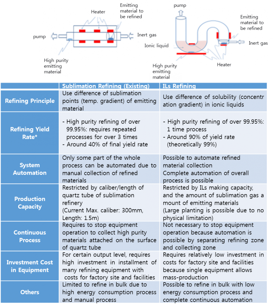
Until now, ‘sublimation refining method’ has been used to get high purify organic light-emitting material by utilizing the difference of sublimation points between vaporization and solidification of a material. However, cons of this method are low yield rate and very high production cost because it is impossible to realize complete auto and continuous process.

To address this issue, Dr. Kim’s team started developing the large scale refining technology for the organic light-emitting materials at low cost since 2011 and applied for original patent in December, 2012. Their effort on verifying the possibility of the technology’s application produced this result in 19 months.

The key of the result is the application of the high purity refining technology on the organic light-emitting material for the OLED TV by focusing on the non-volatile feature of ILs at high vacuum·high temperature.

This technology uses a principle of separating impurities in the order of vaporizing the organic light-emitting material in a vacuum chamber; dissolving it in a liquid filter of ionic liquid; and recrystallizing supersaturated material in the liquid. It enables to get 99.95% of high purity organic light-emitting material through one refining process.

It is a completely new concept of large scale refining method based on the non-volatility characteristic of ionic liquid at high vacuum·high temperature.

The team is credited with the success of new technology development which can overcome the cons of the existing sublimation refining method including refinery yield rate, automation and continuous process of equipment, and efficiency of mass production. It is also expected to bring a huge cost reduction effect by recycling; collect and reprocess during refinery process, of the expensive but non-volatile ionic liquid.

According to “2014 OLED Emitting Material Annual Report Market Forecast (~2020)” by a professional OLED market research firm, UBI Research, the OLED emitting material market is expected to grow to 1.3 trillion won in 2017 from 2014 estimation of 543 billion won. Forecasted annual growth rate is over 30% and experts see that the growth will be much larger if large size display market including the AMOLED TV expends in full-scale.

Dr. Taewon Kim, said, “this technology increased the yield rate and decreased the production cost by more than 50%. And an ultimate goal is to reduce the current price by one tenth” and “technology development is in progress with companies.” He also said, “the success is a game changer with enormous potential to turn the OLED TV market-to-explosively grow” and “based on the low-cost and large scale refining original technology, domestic businesses will largely contribute to preoccupy the global market of forward-backward industry regarding the OLED TV.”

The team currently applied 16 cases for patent with related process․equipment technology in and out of the country and plans active technology transfer to related businesses.
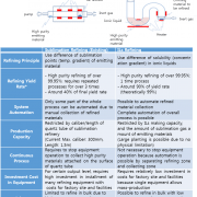
<Comparison of refining methods for organic light emitting materials Source: KITECH>