Posts

[IMID 2017] Opening solution for next generation high-resolution OLED implementation

Various solutions for high resolution OLED implementation were released at iMiD 2017 held in COEX from October 18th to 19th. As the resolution of small and mid-sized OLEDs, which are currently being commercialized, is staying at the QHD level, the solutions released at this time have attracted a great deal of attention from display members.

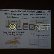
First, Hwang Chang-hoon, CEO of OLEDON, who is developing plane source FMM deposition technology, announced at the business forum, “The plane source FMM deposition technology currently being developed is the only alternative for ultra-high resolution OLED manufacturing at 2,250 ppi”. Hwang Chang-hoon CEO said, “We measured the shadow distance using a-step, and it was 0.38 μm. We can fabricate OLED device with 2,250 ppi only if we have this shadow distance.” “We are currently looking for shadow-free process conditions”
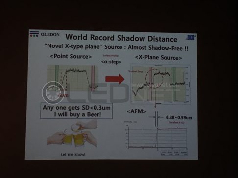
<Difference in shadow distance between point source and plane source>

In addition, Hwang Chang-hoon said, “We first co-deposited the host material and the dopant material on the metal plate to evaporate the deposited green donor thin film and measure the green target thin film with the same PL wavelength for the first time” and “Color control of target thin films made with plate sources can be controlled by the amount of dopant molecules in the donor film, so color control is expected to be easy”.
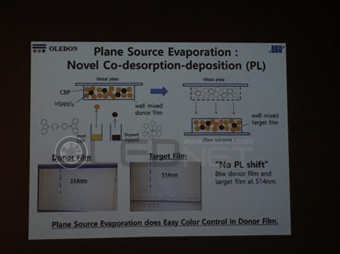
<OLEDON plane evaporation co-deposition material>

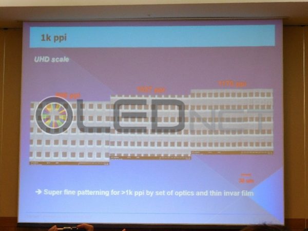
AP Systems, which recently announced the successful development of 1,000 ppi FMM using ultra-short pulse laser (USPL), exhibited 5.28 inch FMM of 825 ppi and 4.72 inch FMM of 677 ppi at this exhibition. A company official said, “By developing a burr-free laser process to solve the burr problem caused by the heat generated during the fabrication process, it is possible to fabricate not only FMM of 1170 ppi but also FMM of various shapes”.
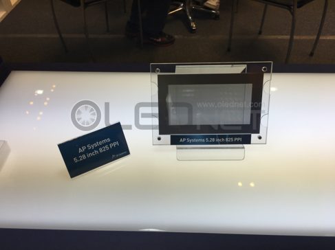
<5.28 inch 825ppi FMM of AP Systems>

Finally, Philoptics unveiled FMMs fabricated using electro forming, especially, FMM of 1,200 ppi, which attracted attention this time, was displayed separately in the VIP room. A company official said “We have secured the stability of the process for the production of 1,200 ppi FMM,” and mentioned “We plan to deliver it to panel makers for testing in the first half of next year, and aim to develop FMM at 2,000 ppi later.”
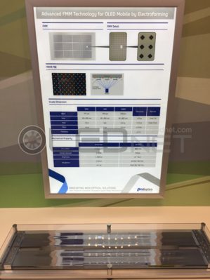
<FMM of Philoptics manufactured by electro forming method>

As such, in this iMiD 2017, various solutions for high-resolution patterning of OLEDs has been released. Recently, as the number of contents requiring high-resolution OLED such as virtual reality contents increases, interest of smartphone users are increasingly interested. It is worth noting which solution will enable the small to medium-sized UHD OLED era.

[IMID 2017] 차세대 고해상도 OLED 구현을 위한 solution 대거 공개

지난 10월 18일부터 19일까지 코엑스에서 열린 iMiD 2017에서 고해상도 OLED 구현을 위한 다양한 solution들이 공개 됐다. 현재 상용화 되고 있는 중소형 OLED의 해상도가 QHD급에서 머물고 있는 만큼 이번에 공개 된 solution들은 디스플레이 관계자들에게 큰 주목을 받았다.

먼저, 면소스 FMM 증착 기술을 개발 중인 OLEDON의 황창훈 대표는 business forum에서 “2,250 ppi의 초고해상도 OLED 제조를 위해서는 현재 개발 중인 면소스 FMM 증착기술이 유일한 대안”이라고 발표하였다. 황창훈 대표는 “a-step을 이용하여 shadow distance를 측정한 결과 0.38 um였으며, 이러한 shadow distance를 가져야 비로소 2,250 ppi의 OLED 소자 제작이 가능하다”라며 “현재 shadow-free한 공정 조건을 찾고 있다”라고 밝혔다.

<포인트소스와 면소스의 shadow distance 차이>

또한, 황창훈 대표는 “호스트 물질과 도판트 물질을 금속면에 co-deposition하여 증착된 그린 도너박막을 재증발하여 동일한 PL 파장을 가지는 그린 타겟박막을 최초로 측정하였다”며 “면소스로 제작한 타겟박막의 칼라 제어는 도너박막의 도판트 분자의 양으로 조절이 가능하기 때문에 색 조절이 쉬울것으로 예상된다”라고 밝혔다.

<OLEDON의 면증발 co-deposition 자료>

한편, 최근 USPL(ultra-short pulse laser)을 이용하여 1,000 ppi FMM 개발에 성공했다고 발표한 AP Systems는 이번 전시회에서 825 ppi의 5.28 inch FMM와 677 ppi의 4.72 inch FMM을 전시했다. 업체관계자는 “burr-free laser process를 개발하여 제작 공정 시 발생하는 열로 인한 burr 문제를 해결하였으며, 이러한 방식으로 1170 ppi의 FMM 뿐만 아니라 다양한 형태를 갖는 FMM도 제작이 가능하다”고 언급했다.

<AP Systems의 5.28 inch 825ppi FMM>

마지막으로 Philoptics는 전해주조(electro forming)을 이용하여 제작 된 FMM들을 공개하였으며, 특히 이번에 주목받은 1,200 ppi의 FMM은 VIP room에 따로 전시하였다. 업체 관계자는 “현재 1,200 ppi FMM 제작을 위한 공정의 안정성도 확보했다”고 밝히며 “내년 상반기에 test용으로 패널 업체에 납품 예정이며 추후에 2,000 ppi 수준의 FMM을 개발하는 것이 목표”라고 언급했다.

<전해주조 방식으로 제작 된 Philoptics의 FMM>

이처럼 이번 iMiD 2017에서는 OLED의 고해상도 패터닝을 위한 다양한 solution이 공개 됐다. 최근 들어 가상현실 컨텐츠 등 고해상도 OLED가 필요한 컨텐츠들이 증가함에 따라 스마트폰 사용자들의 관심도 점점 고조되고 있다. 중소형 UHD OLED 시대는 어느 solution에 의해 개화 될지 귀추가 주목된다.

[iMiD 2017] JOLED announces printing-type OLED development trend and future road map

At the ‘IMID 2017 Business Forum’ held in COEX, Seoul from 18th to 19th, Toshiaki Arai, chief technologist of JOLED announced JOLED’s printing technology and future road map.

<JOLED’s Toshiaki Arai chief technologist>

Toshiaki Arai, chief technologist stated that a stable jetting technology at 220 ppi level has been currently secured; high resolution OLED with more than 300 ppi has been developed at Gen 8.5 but there are some issues such as jetting accuracy and stability.

Toshiaki Arai introduced TG-TAOS (top gate-transparent amorphous oxide semiconductors) TFT, which will contribute to saving the unit cost of OLED with excellent performance at low price.

He also announced the future strategy of JOLED, stressing that, instead of small and large OLED dominated by South Korean companies, the middle-sized OLED for tablet and monitor with more than 200 ppi. Joled is the only OLED panel maker that unveiled its 21.6 inch 4K RGB OLED in 2017, using printing process, and has pilot launched.

<JOLED’s 21.6 inch 4K OLED in application of printing method>

On the other hand, according to the Nihon Keizai newspaper in Japan, JOLED is reported to have invested 100 billion yen in mass production of printing-type OLED. In addition, Toshiaki Arai stated that the OLED test samples manufactured by printing process have been provided since this April and the mass production will realize in the second half of 2018.

[IMID 2017] JOLED, printing 방식의 OLED 개발 동향과 미래 로드맵 발표

지난 18일부터 19일까지 서울 코엑스에서 열린 ‘IMID 2017 Business Forum’에서 JOLED의 Toshiaki Arai chief technologist는 JOLED의 printing 기술과 향후 로드맵 등을 발표하였다.

<JOLED의 Toshiaki Arai chief technologist>

Toshiaki Arai chief technologist는 현재 220 ppi 수준에서 안정적인 jetting 기술을 확보하였다고 밝히며, Gen 8.5에서 300 ppi 이상의 고해상도 OLED도 개발하고 있으나 jetting 정확도와 안정성 등의 이슈가 있다고 언급했다. 이어서 printing OLED에 적용 될 TG-TAOS(top gate-transparent amorphous oxide semiconductor) TFT를 소개하며 낮은 가격으로 충분한 성능을 발휘하기 때문에 OLED 원가 절감에 기여할 것이라고 밝혔다.

이어서 Toshiaki Arai chief technologist는 JOLED의 미래 전략을 소개하며 한국 기업이 주도하고 있는 소형과 대형 OLED 대신 200 ppi 이상의 tablet과 monitor용 중형 OLED에 먼저 집중할 것을 밝혔다. JOLED는 OLED panel 업체 중 유일하게 2017년에 printing 공정을 이용하여 21.6 inch 4K RGB OLED를 공개하였으며 이를 시험 출하 하기도 하였다.

<Printing 방식을 적용한 JOLED의 21.6 inch 4K OLED>

[iMiD 2017] Samsung Display, OLED를 이용한 application 대거 공개

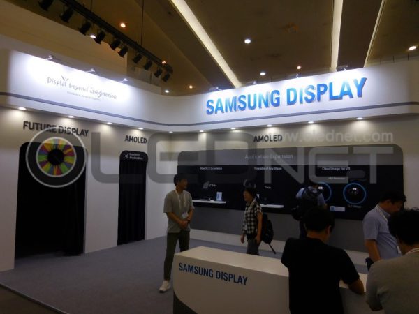
Samsung Display는 지난 8월 28일부터 31일까지 부산 벡스코에서 열린 iMiD 2017에서 VR과 light field display 등 OLED를 이용한 다수의 application을 대거 공개하며 큰 주목을 받았다.


<Samsung Display 부스>


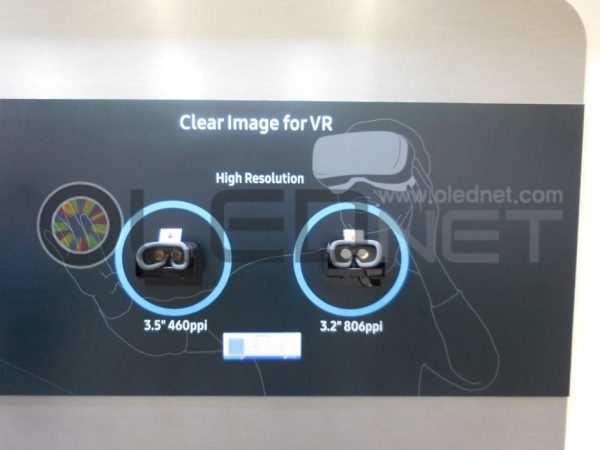
먼저, Samsung Display는 가상현실용 460ppi 해상도의 3.5 inch OLED와 806ppi 3.2 inch OLED를 비교 전시하였다. 업체 관계자는 “ppi가 높을수록 더 향상 된 현실감과 몰입감을 체험할 수 있다.”며, “현재 더 높은 해상도의 OLED가 개발 중이다”고 언급했다.


<3.5 inch 460 ppi OLED와 3.2 inch 806 ppi 비교>


또한, Samsung Display는 future display zone에서 OLED light field display를 전시하였으며, AMOLED zone 에서는 관람객들이 LCD와 OLED를 직접 비교할 수 있는 자리를 마련하였다.

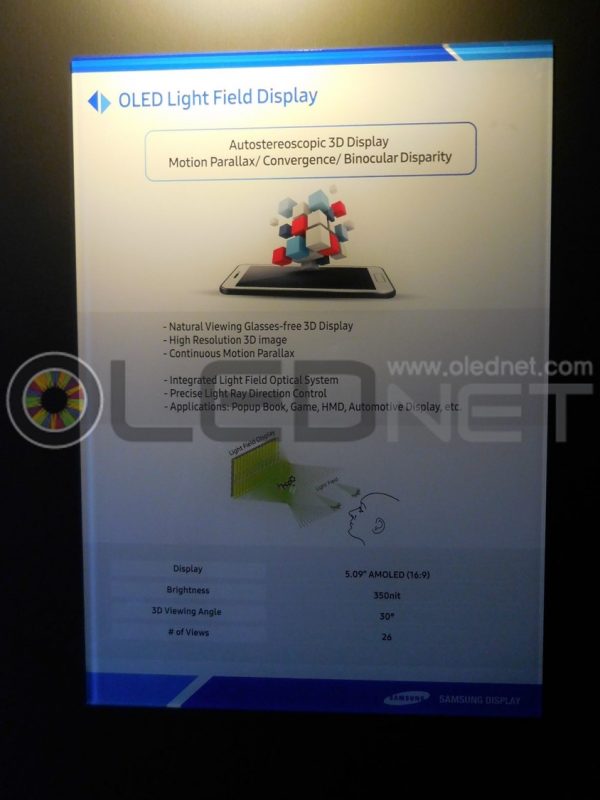
업체 관계자는 light field display에 대해 “패널 위에 광학 렌즈를 적용하여 3D를 구현한 기술로서 빛의 간섭효과를 이용한 홀로그램과는 조금 다른 방식”이라고 설명하였다. 또한,  “30° 보다 더 넓은 viewing angle 개발 중”이라며 “현재 pixel과 렌즈 정렬 문제와 광학 설계 등의 이슈가 있다”고 밝혔다.


<OLED light field display 설명과 사양>


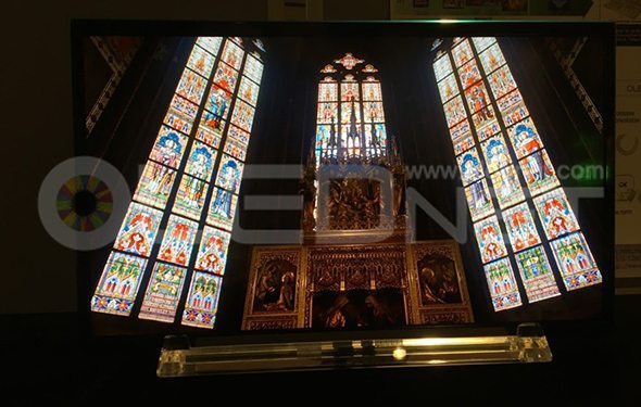
AMOLED zone에서는 LCD와 OLED의 명암비를 직접 비교 체험할 수 있도록 패널들을 전시하였다. OLED의 명암비와 색표현력은 LCD 대비 명백한 차이를 보였으며, 업체 관계자는 “이러한 차이가 Galaxy 시리즈에 OLED가 사용 되고 있는 이유”라고 언급했다.


<OLED(좌)와 LCD(우) 화질 비교>


Samsung Display는 그 외에도 1.3 inch circle OLED와 12 inch FHD OLED 등을 선보이며 전시회 기간 동안 관람객들의 큰 관심을 이끌었다.

[iMiD 2017] Samsung Display, Huge release of application using OLED

Samsung Display has received great attention by releasing a large number of applications using OLED such as VR and light field display in iMiD 2017 held in BEXCO, Busan from 28th to 31st August.


<Samsung Display booth>


First, Samsung Display comparatively exhibited a 3.5-inch OLED with 460ppi resolution for virtual reality and an 806ppi 3.2-inch OLED. A company official said “The higher the ppi, the better the experience of realism and immersion,” and mentioned “We are currently developing higher resolution OLEDs.”


<Comparison of 3.5 inch 460 ppi OLED and 3.2 inch 806 ppi>


In addition, Samsung Display exhibited OLED light field displays in the future display zone, and in the AMOLED zone, visitors can directly compare LCD and OLED.

A company official explained that “light field display is a technology that implements 3D by applying an optical lens on a panel, which is a little different from hologram using light interference effect.” And he said “We are developing a viewing angle that is wider than 30 °,” revealed “We now have pixel and lens alignment issues and optical design issues.”


<OLED light field display description and specification>


In the AMOLED zone, panels were displayed to directly compare the contrast ratio of LCD and OLED. The contrast ratio and color expressiveness of the OLEDs were clearly different from those of the LCDs, and a company official said, “These differences are the reasons why OLEDs are used in the Galaxy series.”


<Comparison of OLED (Left) and LCD (right) image quality>


Samsung Display has also introduced 1.3 inch circle OLED and 12 inch FHD OLED, which led to the great interest of the visitors during the exhibition.

[iMiD 2017] LG Display, Spur Development of 77 inch transparent flexible OLED

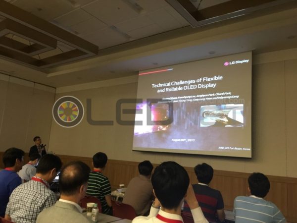
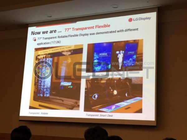
LG Display’s Kwon Se-Yeol senior researcher introduced the 77-inch transparent flexible OLED which had been introduced in June at IMID 2017 held in BEXCO, Busan on Aug. 30, and announced the applied technologies to realize this.


Kwon Se-Yeol senior researcher mentioned, “OLED is self-luminous, so it can be manufactured with a thin thickness because it does not need a back light unit. The thinner the thickness, the more flexible the OLED can be so that it is easy to implement flexible displays with OLEDs.” and forecasted. “It can be used in various fields such as signage and smart desk.”


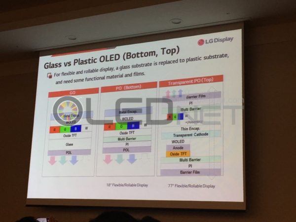
The 77-inch transparent flexible OLED which is released this time is a top emission type for improved luminance. The transparent thin film encapsulation layer is applied, different from the conventional OLED TV or large flexible OLED, and two polyimide substrates are used.


Kwon Se-Yeol senior researcher said “We applied a transparent thin-film encapsulation layer instead of the existing metal encapsulation layer for the top emission method ” and explained “A white OLED light emitting layer and a color filter layer were formed on two polyimide substrates and cemented together. A barrier film and a multi-barrier were applied to the top and bottom of the polyimide substrates to prevent moisture and oxygen penetration.”


The Kwon Se-Yeol senior researcher then states that “flexural rigidity of the panel is mainly affected by the thickness of the polarizer and the encapsulant layer, so it is necessary to reduce the thickness in order to improve the flexibility”, and emphasized “By reducing the thickness of the encapsulant layer from 100 μm to 20 μm, we can reduce the strain on the OLED module from 0.36% to 0.21%, along with improved flexibility”.

In addition, he mentioned that surface reflection due to polyimide birefringence phenomenon, laser wavelength selection according to polyimide properties in LLO (laser lift off) process, and use of flexible OLED module are all covered, and technical development is continuing.

Meanwhile, LG Display has developed the world’s first 77-inch transparent flexible OLED with UHD (3840 × 2160) resolution, transmittance of 40%, and radius of curvature of 80R as part of the national project.

[iMiD 2017] LG Display, 77 inch 투명 플렉시블 OLED 개발 박차

LG Display의 권세열 책임은 8월 30일 부산 벡스코에서 개최중인 IMID 2017에서 지난 6월 선보인 77 inch 투명 플렉시블 OLED를 소개하며 이를 구현하기 위해 적용 된 기술들을 발표하였다.


권세열 책임은 “OLED는 자발광이라 back light unit이 필요 없어 얇은 두께로 제작이 가능하며, 두께가 얇을 수록 유연성이 향상 되기 때문에 OLED는 플렉시블 디스플레이를 구현하기 용이하다”고 언급하며 “추후 사이니지와 스마트 책상 등 여러 분야에서 적용이 될 수 있을 것”이라 전망했다.


이번에 공개 된 77 inch 투명 플렉시블 OLED는 휘도 향상을 위한 전면 발광방식으로, 기존의 OLED TV나 대형 플렉시블 OLED와는 다르게 투명박막 봉지층이 적용되었으며 polyimide 기판이 2장 사용 되었다.

권세열 책임은 “전면 발광방식을 위해 기존의 금속 봉지층 대신 투명 박막 봉지층을 적용하였다”고 밝히며 “2장의 polyimide 기판에 각각 white OLED 발광층과 칼라필터층을 형성하여 합착 하였다. polyimide 기판 상하부에는 수분과 산소 침투를 방지하기 위해 barrier film과 multi barrier가 적용 되었다”라고 설명했다.


이어서 권세열 책임은 “패널의 휨 강성(flexural rigidity)는 주로 편광판과 봉지층 두께의 영향을 받기 때문에 유연성을 향상시키기 위해서는 두께를 줄이는 것이 필수”라며 “봉지층의 두께를 100um에서 20um까지 줄이면 유연성 향상과 함께 OLED 모듈에 가해지는 변형율(strain)도 0.36%에서 0.21%까지 저감할 수 있을 것”이라 강조하였다.

그 밖에 polyimide 복굴절 현상으로 인한 표면반사이슈와 LLO(laser lift off) 공정 시 polyimide 성질에 따른 laser의 파장 선택, 유연성을 가지는 OLED 모듈 사용 등의 주요 이슈를 다루며 기술 개발이 지속적으로 이루어지고 있다고 언급했다.

한편, LG Display는 국책과제의 일환으로써 UHD(3840 × 2160) 해상도와 투과율 40%, 곡률반경 80R을 가지는 77 inch 투명 플렉시블 OLED를 세계 최초로 개발한 바 있다.

[iMiD 2017] AP Systems, USPL을 통해 FMM의 해답을 찾다

28일 부산 BEXCO에서 개최된 iMiD 2017에서 AP Systems는 USPL(ultra-short pulse laser)로 1000ppi FMM개발에 성공했다고 발표하였다.

FMM은 화소와 RGB 유기물을 증착하는 역할을 하기 때문에 FMM은 OLED의 해상도와 수율을 결정짓는 요소로서 작용된다. 현재 FMM은 주로 전주(etching) 방식으로 제작되고 있다. 이 방식은 미세 패턴의 정밀도와 두께, 무게에 의한 섀도우 현상이 발생하는 문제가 있어, 이를 해결하기 위해 laser 가공, 전해주조(electro-forming)등 다양한 FMM 제조 공정이 개발되고 있다.

이 중 laser 가공 방식은 laser 조사 시 발생하는 열(thermal effect)로 인해 pin-hole 주변에 burr가 형성되는 이슈가 있다. 이러한 burr는 FMM의 섀도우 구간을 증가, RGB 유기물 증착 시 패턴이 겹치는 현상을 야기시킴으로써 OLED의 해상도를 저하시킨다.

AP Systems는 이러한 점을 착안해 burr 현상이 없고, 나아가 taper angle을 제어하는 burr-free laser process을 개발하였다.

Burr-free laser process는 단방향 펄스를 일정 횟수로 나누어 짧게 조사하는 방식으로 연속적으로 laser를 조사하지 않기 때문에 축적되는 열 에너지가 최소화 되어 burr 형성을 막는다. 또한, laser의 energy를 제어함으로써 energy 축적하여 taper를 형성하는 방식이다.

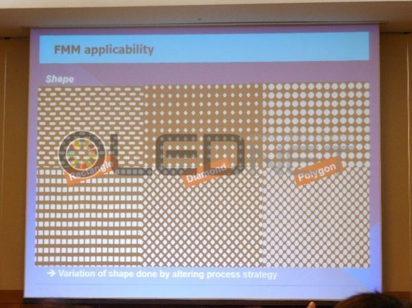
AP Systems는 이 방법을 통해 ‘1170ppi의 FMM 뿐만 아니라 미세 pin-hole의 모양이 사각형 또는 다이아몬드, 다각형 등 다양한 형태를 갖는 FMM도 제작하였다’며 ‘USPL 방식이 적용된 대면적 FMM 제조 장비도 개발하였다’고 설명하였다.

또한, AP Systems는 FMM 제조 장비에 대해 ‘multi-beam과 USPL이 장착되어 있어 생산성을 향상시킬 수 있으며, UHD를 구현할 수 있다’고 덧붙였다.

14년 Galaxy Note4 출시 이후부터 아직까지 OLED의 해상도는 QHD 급에 머물고 있다. 고해상도(UHD급 이상)를 가지는 OLED를 제조하기 위해서는 FMM이 기술적으로 직면하고 있는 다양한 문제를 해결해야 되는 실정이다. 이에 따라 AP Systems의 USPL 기술이 향후 OLED 시장에 어떠한 영향을 미칠지 앞으로의 귀추가 주목된다.

<AP Systems가 제작한 1000ppi FMM>


<다양한 형태의 FMM>

[iMiD 2017] AP Systems, Find FMM answers through USPL

At iMiD 2017 in BEXCO, Busan on 28th, AP Systems announced that it succeeded in developing 1000ppi FMM with USPL (ultra-short pulse laser).

Since FMM plays a role of depositing pixels and RGB organic materials, FMM serves as a factor that determines resolution and yield of OLED. At present, FMM is mainly manufactured by etching method. This method has a problem that a shadow phenomenon due to the precision, thickness, and weight of the fine pattern occurs, in order to solve this problem, various FMM manufacturing processes such as laser processing and electro-forming have been developed.

Among these, laser processing method has an issue of forming burrs around pin-holes due to the thermal effect caused by laser irradiation. These burrs increase the shadow interval of the FMM, which causes overlapping of patterns during RGB organic deposition, thereby degrading the resolution of the OLED.

AP Systems has developed a burr-free laser process that does not have burr phenomenon and further controls the taper angle.

The Burr-free laser process is a short-time irradiation of unidirectional pulses at a constant number of times, since the laser is not continuously irradiated, it minimizes accumulated heat energy and prevents burr formation. In addition, by controlling energy of the laser, it accumulates energy and forms taper.

In this way, AP Systems explained ‘they produced FMM with various shapes of fine pin-holes such as square, diamond, and polygonal shapes, as well as 1170ppi FMM’, and ‘’We also developed large-area FMM manufacturing equipment with USPL method’.

AP Systems also added ‘multi-beam and USPL is equipped for FMM manufacturing equipment so that it can improve productivity and realize UHD’.

Since the launch of the Galaxy Note4 in 2014, the OLED resolution has remained at the QHD level yet. In order to manufacture an OLED having a high resolution (UHD level or higher), it is necessary to solve various technical problems faced by FMM. Accordingly, it is noteworthy how USPL technology of AP Systems will affect the future OLED market.

<1000ppi FMM produced by AP Systems>


<various type of FMM produced by AP Systems>