Posts

QNED (quantum dot nano-rod LED) structure and core technology

Samsung Display research center is accelerating the development of QNED as the next-generation display following OLED.

The reason Samsung Display is developing QNED as part of its large-size display business is that it is the only display that can produce the image quality that Samsung Display’s biggest customer, Samsung Electronics, can satisfy.

Samsung Electronics’ TV business direction, which has the world’s No. 1 TV market share, is to use QD to make color gamut better than OLED, and to use a display that can maximize HDR performance with high luminance and excellent gradation characteristics on a bright screen.

The only display that can satisfy the needs of Samsung Electronics is QNED.

Items QNED OLED Mini-LED LCD
Color gamut best better best
HDR best better better
Luminance best better better
Contrast ratio best best better
Motion blur best best good


QNED is a self-luminous display and because it uses QD, it has the best color gamut, HDR, luminance, contrast ratio, and motion blur, etc., and is a product expected by Samsung Electronics.

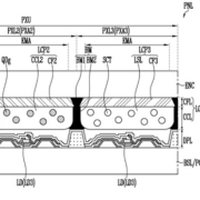
It can be confirmed by the structure that QNED is the display with the best characteristics. QNED consists of a pixel layer with a nano-rod LED on the TFT structure of 3T1C used in large OLEDs, and a color conversion layer consisting of QD and CF (color filter) on top.

In OLED, electrodes (cathode and anode) and electrode line for transmitting a signal to a pixel are located above and below the light emitting material, whereas in QNED, both the signal transmitting electrode (pixel electrode) and electrode line are located on the same plane. In addition to the pixel electrode, the QNED additionally includes a reflective electrode to increase light output efficiency. The pixel electrode serves as an alignment electrode for aligning the nano-rod LED.

< QNED section structure >

< QNED pixel structure >

< QNED pixel planar structure >

Looking at the planar structure of a QNED pixel, a plurality of pixel electrodes are connected in series in one pixel, and a nano-rod LED is positioned between the pixel electrodes. The pixel electrode is on the pixel wall (PW) formed of an insulating material, and each pixel is surrounded by a bank (BNK) to separate regions.


The core technology of QNED is driving technology and sensing technology.

The driving technology includes a driving technique for aligning nano-rod LEDs and a driving technique for uniformly controlling pixels that may have a deviation in the number of nano-rod LEDs. The alignment circuit includes switching elements for each pixel, and the switching element applies an alignment signal to the pixel. The alignment state of the nano-rod LED is determined depending on which alignment signal is given to each pixel.

< Drive circuit for alignment >

< Sensing transistor for checking alignment >

The most important driving technology is a technology that supplies current to each pixel so that the luminance can be uniform across the entire screen even if the number of nano-rod LEDs per pixel is different. It is a method of controlling each pixel based on the data read from the sensing transistor.

[QNED Technology Completion Analysis Report] details the sensing transistor, sensing wiring, and sensing signals that can check the nano-rod LED alignment status on the panel.


As sensing technology, there are sensing technology (sensing transistor) designed inside QNED and sensing technology used in QNED manufacturing. The sensing technology used to manufacture QNEDs is inherent in inkjet systems. There are three sensing technologies in the inkjet system: the number of nano-rod LEDs in the ink and the viscosity analysis of the solvent, the analysis of the number of nano-rod LEDs sprayed on the panel, and the analysis of the nano-rod LED alignment state.

< Inkjet system configuration >


QNED has already proven that 4K 65 inches can be driven two years ago. Samsung Display is concentrating on finishing work to secure the screen uniformity of QNED.
[28TH FINETECH JAPAN] JDI and JOLED, announced Strengthening Cooperation for Mid-sized OLED Market

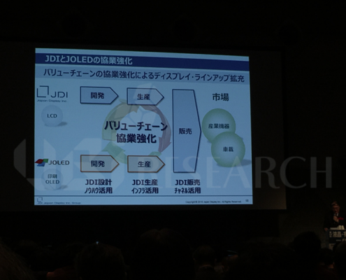
At the 28th FINETECH JAPAN held in Tokyo, Japan from December 5 to 7, 2018, JDI and JOLED announced that they would intensify their cooperation in order to target the middle-sized OLED market.

JDI announced that it will actively promote JOLED’s solution process OLED to medium-sized OLED markets such as industrial display markets or automotive display markets through its own design know-how, production infrastructure, and sales channels,.

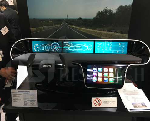
In particular, JDI announced that it will provide new value to next-generation automotive fields along with JOLED such as support for safety such as electronic mirrors and displays for A/B pillars, new interface functions, movie appreciation using 4-8K displays, and the displays that are harmonized with interior design such as curved surfaces and big screens.

JDI and JOLED also shared booths for exhibition. JOLED introduced 21.6-inch FHD OLED monitors for e-sports and medical applications. In addition, it introduced a number of medium-sized OLEDs such as 12.3-inch HD OLED for automobiles, 12.2-inch FHD flexible OLED, 27-inch 4K OLED for home interior, and 21.6-inch 4K flexible OLED with cylindrical form. It also showcased large OLEDs such as 54.6 inch 4K OLED.

On the other hand, JOLED announced in July, 2018 that it would open its Nomi office for mass production of solution process OLED. Based on 5.5 generation glass substrates, Nomi has production capacity of 20,000 glass substrates per month and plans to mass-produce in 2020.

JOLED raised 47 billion yen to spur solution process OLED business for automobiles.

JOLED, the world’s first to successfully commercialize solution process OLED products, announced that it had raised a total of 47 billion yen as a third-party capital increase.

According to JOLED, Denso will invest 30 billion yen, Toyota Tsusho 10 billion yen, Sumitomo chemical 5 billion yen and SCREEN Finetech Solutions 2 billion yen. JOLED is known to cooperate with Denso to develop automotive displays and Sumitomo chemical to develop OLED materials for solution process.

In particular, Denso has been mainly using TFT-LCD for automotive displays, but it is expected to lead the development for applying lightweight and easy-to-shape OLED to automobile interior through this investment.

It is expected that this funding will accelerate the establishment of production system for the mass-production of JOLED’s solution process OLED. JOLED announced on July 1 that it would set up a “JOLED Nomi Office” in Nomi-city, Ishikawa, and aim to operate in 2020.

Major production products are medium-sized (10 to 32-inch) solution process OLEDs that will be used for cars or high-end monitors. Also, Toshiaki Arai, chief technologist of JOLED announced that they would target the middle-sized OLED market with solution process OLED, at the 2018 OLED Korea conference hosted by UBI Research in March.


Inkjet might take advantageous position for Gen11 super large OLED mass production line!

Toshiaki Arai, chief technologist of JOLED and James Lee, deputy chief engineer of TCL made presentations for the solution processed OLED on March 7 at the ‘4th OLED Korea conference’ held at Novotel Ambassador Hotel in Gangnam, Seoul, hosted by UBI Research.

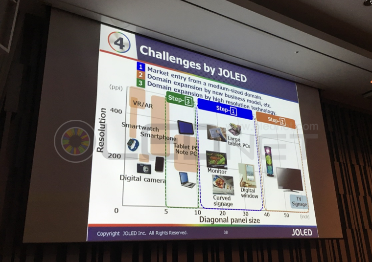
Toshiaki Arai, chief technologist of JOLED announced that JOLED will focus on the medium-size OLED market for 10 ~ 30 inch tablets with solution processed OLED. He explained “OLEDs for mobile devices are currently targeting over 500 ppi and at least 800 ppi, which is hard for today’s printing technology. However, current printing technology is competitive enough since the medium-size OLED for tablets is 300 ppi level”.

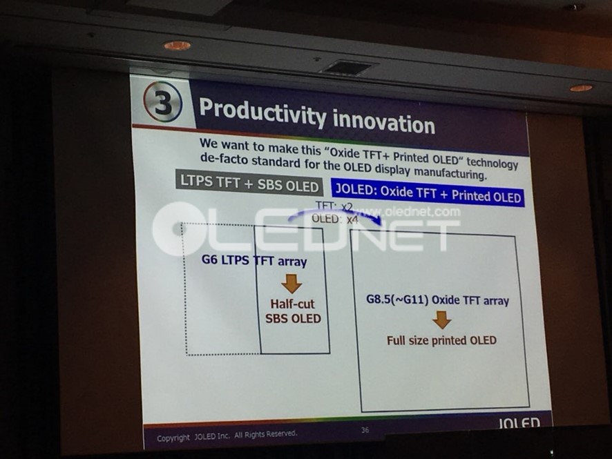
He also added, “While it is required to divide the mother glass with the deposition technology currently in use, JOLED’s oxide TFT and solution process OLED can be adopted to Gen 8.5 as well as Gen 11 without cutting the mother glass. Thus, we expect panel production to be increased significantly.

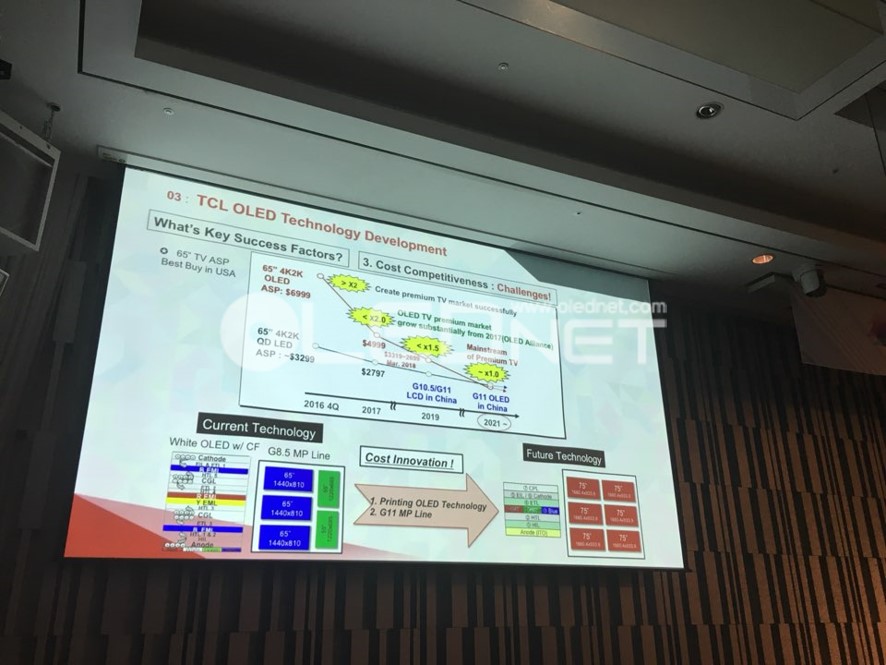
James Lee, deputy chief engineer of TCL commented that the next-generation premium TVs are to implement 70-inch or larger screen, full black representation, high-definition at 8K resolution, and design differentiation such as slim & flexible. He said “solution process technology enables large RGB OLED implementation, which can improve image quality and reduce cost by using less material. TCL is currently developing solution process technology, which might be expected to be applied to its planned Gen 11 factory. ”

He commented “OLED TV prices are now approaching the price of LCD TVs based on 65-inch standards. In 2021, OLED TVs and LCD TVs will not differ in price, and OLED TVs will become the mainstream of the premium TV market. ”

Also he emphasized “Gen11 OLED needs to improve mura (unevenness) free technology, but it can produce six sheets of 75-inch OLED panels, and it is three times the production volume of GEN 8.5, with a cutting efficiency rate of 95% or more. In order for OLED TV to become the mainstream of the TV market, it is necessary to establish Gen 11 solution process OLED factory. ”

Gen11 초대형 OLED 양산라인, inkjet으로 선점!

3월 7일 유비산업리서치 주최로 서울 강남 노보텔앰배서더 호텔에서 열린 ‘제 4회 OLED Korea conference’에서 JOLED의 Toshiaki Arai chief technologist와 TCL의 James Lee deputy chief engineer는 solution process OLED를 주제로 발표를 진행했다.

JOLED의 Toshiaki Arai chief technologist는 solution process OLED로 10~30 inch대 태블릿용 중형 OLED 시장을 집중 공략할 것을 밝혔다. Toshiaki Arai chief technologist는 “mobile 기기용 OLED는 현재 500 ppi를 넘어 최소 800 ppi 이상을 목표로 하고 있어 현재 프린팅 기술로는 힘들다. 하지만 태블릿용 중형 OLED는 300 ppi 수준이기 때문에 현재 프린팅 기술로는 충분히 경쟁력이 있다”고 설명했다.

이어서 “현재 적용 되고 있는 증착 기술은 원장 분할이 필수이지만, JOLED의 oxide TFT와 solution process OLED는 Gen8.5를 넘어 Gen11에서도 원장분할 없이 공정이 가능하기에 패널 생산량도 대폭 확대 될 수 있을 것”이라 전망했다.


TCL의 James Lee deputy chief engineer는 차세대 premium TV는 70 inch 이상의 대형 화면과 완벽한 블랙표현과 8K 해상도의 고화질, slim & flexible 등의 디자인 차별화 임을 언급하였다. James Lee deputy chief engineer는 “solution process 기술이 대형 RGB OLED 구현이 가능하여 화질 향상이 가능하고 적은 재료 사용으로 원가 절감에도 기여할 수 있을 것”이라며, “TCL은 현재 solution process 기술을 개발 중으로 Gen11 공장에 적용이 가능할 것으로 예상된다”고 밝혔다.

이어서 “현재 65 inch 기준 OLED TV 가격이 LCD TV 가격에 근접하고 있다”며 “2021년에는 OLED TV와 LCD TV 가격이 차이가 없을 것이며 OLED TV가 premium TV 시장의 주류로 자리잡을 것”이라 설명했다.

또한, “Gen11 OLED는 Mura free 기술 향상이 필요하지만, 75 inch OLED 패널을 6장 생산이 가능하며 Gen8.5 대비 3배 증가한 생산량과 95% 이상의 면취율이 가능하다”고 설명하며 OLED TV가 TV 시장의 주류로 자리잡기 위해서는 Gen11 solution process OLED 공장 건립이 반드시 필요할 것이라 강조했다.

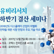
유비리서치 2017년 OLED 결산 세미나: 2018년도 디스플레이 산업의 차별화 전략을 위한 시장 전망과 주요 기술 이슈 세미나 개최

  • 2017년 OLED 시장을 디스플레이 전문 리서치 기관의 분석을 통해 주요 이슈를 되짚어 볼 수 있는 자리 마련
  • 2018년 OLED 산업의 투자 관점, 경제 관점에서 시장을 전망하고 이에 따른 변화 포인트 예측

시장조사 전문 기관인 유비리서치는 2017년 하반기 결산 세미나 12월 7일(목) 서울 삼성동 코엑스 컨퍼런스룸에서 개최한다. 이번 세미나는 ‘2018년도 디스플레이 산업의 차별화 전략을 위한 시장 전망과 주요 기술 이슈’라는 주제하에 2017년 OLED 시장의 주요 이슈를 되짚어 보고 2018년 시장 전망과 변화 포인트를 예측해보는 자리를 마련한다.

2018년 디스플레이 시장은 국내외 디스플레이 업체에서 앞다투어 제품에 OLED를 채택함으로써 매출액 또한 상승곡선을 그릴 것으로 예상하고 있다. TV용 대형 패널 수요가 빠르게 증가하고 있고, 장기적으로 중소형 패널의 수요도 계속 증가될 것으로 기대되기 때문에 전략적 투자 방향은 긍정적으로 평가된다.

이번 세미나는 ‘최근 LG디스플레이의 중국 8.5세대 투자에 대한 이슈’,  ‘삼성 디스플레이의 A5투자가 각 대형디스플레이 패널 시장과 중소형(모바일) OLED패널 시장에 어떤 영향을 미치는지’에 대한 내용으로 신한금융투자 소현철 기업분석부서장이 발표한다.

또한 2018년 가장 주목되는 차세대 Inkjet Printing 기술의 대표 업체 유니젯 김석순 대표가 ‘디스플레이를 위한 잉크젯 프린팅 기술의 개발 역사와 동향’을 발표한다. 스트레쳐블 기술에 핵심 전문가인 고려대학교 홍문표 교수가 현재 기술 개발 상황과 방향에 대하여 심도 있는 발표를 진행한다.

유비리서치 이충훈 대표는 ‘키워드로 돌아보는 2017년 OLED 디스플레이 시장과 2018년 전망’과 ‘중국, 일본 OLED 산업 전망’에 대한 내용으로 2017년을 종합적으로 정리하고 2018년 OLED산업 시장과 기술을 투자 관점, 경제 관점으로 발표한다.

이번 유비리서치 하반기 결산 세미나는 국내 핵심 전문가와 함께 다양한 양질의 정보와 인맥 교류의 장이 형성은 물론 디스플레이 기술의 현황과 미래를 예측할 수 있는 자리가 될 것으로 예상된다. 세미나에 대한 자세한 정보는 공식 홈페이지(http://www.ubiresearch.co.kr/12_sem/)를 통해 찾아볼 수 있다. 또한 사전등록은 12월 6일까지 접수 가능하다.