Posts

Merck, now it is time to consider the refractive index of common layer materials.

At the ‘OLED settlement seminar for the first half of 2022’ held at COEX on June 23, Merck’s Kim Jun-ho, head of research institute, said, “The concept of the refractive index of the emitting layer is often applied to the capping layer on the cathode, but now it is also required for HTL” and mentioned that the light extraction efficiency can be improved through the optimized refractive index design of HTL.

Next, Kim said, “Because the refractive index of HTL has a trade-off relationship with the hole transport capacity, it is difficult to adjust the refractive index,” and “Even though it was lowered to 1.77 from 1.85, the light extraction efficiency could be improved by 7% without an increase in the driving voltage or a decrease in electron mobility.”
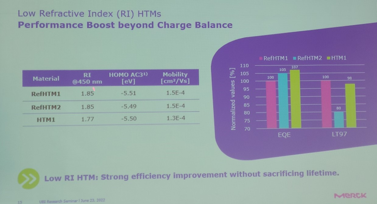
Recently, panel makers are continuously developing the OLED light extraction efficiency. This is because by increasing the light extraction efficiency, as a result, the battery life can be increased. Representative examples include a high-refractive capping layer and micro lens array, and an on-cell film that removes the polarizer and uses a color filter.
The concept of the refractive index of the light emitting, which had been concentrated on the capping layer, is extended to the common layer, and it is expected that panel makers will intensify technological competition, and that there will be many changes in the supply chain of emitting materials of panel makers in the future.
 

Merck’s Blue Ink Material Lifetime Announced 65% Improvement Year-over-Year.

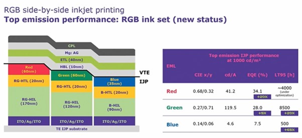
At ‘Display Insight 2021’ held online on November 4th, ‘Joachim Kaiser’, global application manager of Merck, presented ‘Our OLED solutions – livilux®’. When presenting the ink portion of livilux’s OLED materials, Kaiser noted that “Inkjet printing is the only technology that combines RGB parallel pixel layout with scalability for large display sizes”.

Kaiser announced “Maximizing the performance of IJP devices requires a thorough understanding and optimization of state-of-the-art OLED materials, ink formulations optimized for each application, and the entire device stack” and “Merck can get a lot of benefits from IJP performance improvement from its experience in developing materials for deposition”.

Comparing the performance announced by Merck last year and this year, the luminous efficiency (cd/A) of red increased by 46% compared to the previous year, green by 10%, and blue did not change. External quantum efficiency (EQE) was 34.1%, increased by 20% for red, and 28%, increased by 5% for green, and there was no change in blue like the luminous efficiency. In terms of lifespan, 20% for green and 65% for blue were greatly improved. The lifespan of the red is 4,000 hours based on LT95 (last year’s red’s lifespan was 8,300 hours based on LT95), and it is being optimized to increase the lifetime reduced by improving efficiency.

Kaiser emphasized, “At Merck, we are constantly working to provide solutions to the problems of OLED panel design, such as improving the efficiency of Blue OLED, a new kind of emitter, and RGB side-by-side printing technology.”

OLED material makers, why are they going to China?

Recently, OLED material makers are seeking to establish their R & D centers in China.

According to the industry sources, LG Chemical is considering to establish OLED material technology center in Chengdu, China. Merck also announced on June 20 that it will establish its OLED Technology Center in Shanghai, China.

An official from Merck said, “By establishing OLED Technology Center in China, we expect to shorten the product launch period since close cooperation with Chinese companies is possible.In addition, the center will be used as a joint workplace for creating ideal solutions with Chinese companies since it is located in Shanghai.”

This trend of OLED material makers is interpreted as aiming at the growing Chinese market.

If they build their base in China, it will be easy to use the localization strategy specialized in the Chinese market and to secure their suppliers.

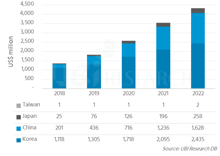
According to UBI research, the OLED market in China will grow at a CAGR of 75%, four times faster than Korea, which is currently the largest market.

In the ‘2018 OLED Emitting Material Industry Report’ issued in June, UBI predicts “ While Korean OLED emitting material market will grow at a CAGR of 21%, China’s OLED material market is expected to grow at a CAGR of 69%, to about US$ 1.16 billion in 2022. This will account for about 38% of the total OLED material market.”

<Emitting material market forecast by country, source: UBI Research>

OLED 재료업체, 중국으로 가는 까닭은

최근 OLED 재료업체가 중국에 R&D센터를 설립하는 방안을 모색하고 있다.

업계에 따르면, LG화학은 중국 청두에 OLED 재료 테크 센터를 설립하는 것을 검토중인 것으로 알려졌다. Merck 또한 지난 20일 상하이에 OLED Technology Center China를 설립한다고 발표했다.

Merck의 관계자는 ‘OLED Technology Center China 설립을 통해 중국 업체들과의 긴밀한 협력이 가능하기 때문에 제품 출시 기간을 단축시킬 수 있을 것으로 기대된다’고 밝혔다. 또한, ‘해당 센터는 상하이에 위치함으로써 중국 업체들과 이상적인 솔루션을 창출할 수 있는 공동 작업 공간으로 활용될 것’이라 말했다.

OLED 재료업체들의 이러한 행보는 점차 커져가는 중국 시장을 공략하기 위한 것으로 해석된다. 중국에 거점을 구축할 경우, 중국 시장에 특화된 현지화 전략을 구사가 용이하고 공급업체를 확보하는데 유리하기 때문이다.

유비리서치에 따르면, 중국의 OLED 시장은 매출액 기준 연평균 75% 성장하고 이는 현재 가장 큰 시장인 한국 대비 4배 이상 빠르다.

또한, 6월 발간한 ‘2018 OLED 발광재료 산업 보고서’에서 유비리서치는 ‘한국의 OLED 발광재료 시장이 연평균 21%씩 성장하는데 반해, 중국의 OLED 발광재료 시장은 연평균 69%씩 성장하여 2022년 약 16.1억달러에 이를 전망이다’고 설명했다. 이는 전체 OLED 발광재료 시장의 약 38% 수준이다.

<국가별 발광재료 시장 전망, 출처:유비리서치>

Merck, Started research on ELQ-LED, a new high-efficiency OLED using quantum materials

Merck said it has begun research on electroluminescent quantum materials-based light-emitting diodes (ELQ-LED) that combine quantum materials in OLED. The project, funded by the German Federal Ministry of Education and Research (BMBF) for a total amount of € 5.5 million, is to develop quantum materials for the display and lighting industries, with a total budget of € 9.1 million.

According to Merck, ELQ-LED, which uses quantum materials in OLED, can achieve high color purity and high energy efficiency at low production costs. However, the use of cadmium, a toxic substance in the quantum materials, has been ruled out. “ELQ-LED shows a systematic improvement in OLED and offers great potential for synergy between OLEDs and quantum materials,” said Michael Grund, Merck’s director of OLED and quantum materials.

Merck, OSRAM OLED, Fraunhofer Applied Polymer Research Institute and University of Augsburg are expected to participate in the project, and Merck will test and develop components, processes, matrix materials, transport materials and inks.

Merck announced that all components would be developed as print materials to save production costs, and printed parts would be tested on displays and automotive tail lamps.

The research project is scheduled to run for three years until the summer of 2020.

Merck, 양자 물질을 이용한 새로운 고효율 OLED인 ELQ-LED 연구에 착수

Merck는 OLED에 양자 물질을 혼합한 ELQ-LED(electroluminescent quantum materials-based light-emitting diode) 연구에 착수 했다고 밝혔다. 독일 연방 교육 연구부(BMBF)로부터 총 550만 유로의 자금을 지원받는 것으로 알려진 이 프로젝트는 디스플레이와 조명 산업을 위한 양자 재료를 개발하는 것으로써 프로젝트의 총 예산은 910만 유로이다.

Merck는 OLED에 양자 물질을 적용한 ELQ-LED가 낮은 생산 비용으로 고색순도와 고에너지 효율 구현이 가능할 것이라고 밝혔다. 다만, 양자 물질 중에서 독성 물질인 카드뮴의 사용은 배제되었다. Merck의 OLED 및 양자 재료 책임자인 Michael Grund는 “ELQ-LED는 OLED의 체계적으로 개선 된 모습을 보여주고 OLED와 양자 재료 사이의 시너지를 위한 큰 가능성을 제시한다.”고 밝혔다.

이 프로젝트는 Merck와 OSRAM OLED, 프라운호퍼 응용 폴리머 연구소, 아우크스 부르크 대학교 등이 참여 할 것으로 알려졌으며, Merck는 구성 요소와 프로세스, 매트릭스 재료, 운송 재료(transport materials), 잉크를 테스트 하고 개발할 예정이다.

Merck는 모든 구성 요소들이 생산비 절약을 위해 모두 인쇄 재료로 개발 될 것이라 밝혔으며, 인쇄 된 부품은 디스플레이와 자동차 테일 램프 부분에서 테스트 될 예정이라 언급했다.

이 연구 프로젝트는 2020년 여름까지 3년 동안 진행 될 예정이다.

Solution Process OLED, Max. 40% Decrease in Component Material Cost Possible Compared to WRGB

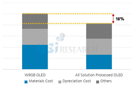
According to 2017 Solution Process OLED Annual Report published by UBI Research, when solution process (ink-jet printing) is applied to large area OLED, it could reduce up to 40% of component material cost, and approximately more than 18% of production cost compared to WRGB process that uses evaporation method.


Solution process is a technology that can manufacture RGB pixel structure of large size OLED panel without cutting mother glass using Gen8 manufacturing equipment or larger.


UBI Research analyst Hyunjun Jang explained that the solution process applied OLED has a simpler panel structure with 5 layers compared to 20 layers of WRGB OLED. WRGB OLED process material usage efficiency is only at 40% but solution process application could increase this to over 90%. Jang added that the lack of color filter is a factor that could decrease panel production price by reducing development cost. Particularly, this can greatly reduce emitting materials usage which occupies much of materials cost and contribute considerably to the fall in production cost. Furthermore, he added that cost setting of soluble emitting material per gram will be an important factor in production cost decrease and emphasized that organic material usage greatly decreases when soluble emitting materials are used but must consider price increase due to solvent cost, production cost, and development cost.


Solution process technology continues to receive attention as a key technology that can lead popularization of large area OLED, and key AMOLED panel companies are carrying out development.


In terms of technology, solution process OLED has lower emitting efficiency and short lifetime as diverse solvent is added to existing evaporation materials to transform into ink leading to low purity. This has been an important issue for panel and material companies for past several years. To improve this, DuPont, Merck, Sumitomo Chemical and others have been actively developing soluble OLED emitting materials. Much like evaporation materials, blue materials showed particular difficulty in performance improvement. However, at present significant portion of technology development has been carried out and investigation shows approximately 80% of lifetime and efficacy of has been achieved compared to evaporation materials.


2017 Solution Process OLED Annual Report compared and analysed WRGB OLED and solution process OLED’s competitiveness in terms of process, materials, and cost. Key issues, soluble OLED emitting materials development status, key companies’ trend, and solution process OLED market are analysed from various perspectives.

<Source: WRGB OLED and solution process OLED production cost comparison, UBI Research 2017 Solution Process OLED Annual Report>

Solution Process OLED, WRGB 보다 최대 40% 부품소재비용 절감 가능.

유비리서치에서 발간한 “2017 Solution Process OLED Annual Report”에 따르면 solution process(ink-jet printing)공정을 대면적 OLED에 적용시 현재 양산에 사용중인 증착방식을 적용한 WRGB 공정대비 최대 40%의 부품소재 비용, 약 18%이상의 제조원가 절감 가능성이 있는 것으로 분석했다.

Solution process는 대면적 OLED panel을 Gen8 이상의 장비에서 원장 분할 없이 RGB pixel 구조로 제조할 수 있는 기술이다.

유비리서치 장현준 선임연구원은 “Solution process가 적용된 OLED는 20 Layer 적층구조로 이루어진 WRGB OLED에 비해 5 Layer만으로 이루어져 패널 구조가 단순하다. WRGB OLED 공정은 발광재료 사용 효율이 약 40%에 불과한데 반해 Solution process 적용시 90% 이상으로 발광재료 사용 효율을 향상시킬 수 있다. 따라서 발광재료 사용량을 크게 감소시킬 수 있어 원가절감에 큰 기여를 할 것으로 기대된다. 또한 color filter를 사용하지 않는 것 또한 패널 제조 원가를 감소 시킬 수 있는 요인이다”라고 언급하였다. 이에 덧붙여 “ Soluble 발광재료 kg당 가격책정이 “원가절감”에 중요한 부분이 될 것이며, soluble 발광재료 사용시 유기재료 사용량은 크게 감소 하지만 solvent 비용과 제조비용, 개발비용으로 인한 가격상승 역시 고려해봐야 할 점”이라고 강조했다.

Solution Process 공정기술은 대면적 OLED의 대중화를 이끌 수 있는 핵심 기술로서 지속적으로 주목받고 있으며 주요 AMOLED panel 업체들 개발을 진행 중에 있다.

기술적인 관점에서 보면 solution process OLED는 기존 증착재료를 ink화 시키기 위해 다양한 solvent를 섞는다. 이때문에 증착재료보다 순도가 낮아 발광효율이 떨어지고 수명이 낮다. 이는 지난 몇 년간 panel 업체들과 재료업체들의 주요 과제였으며 이를 개선하기 위해 DuPont과 Merck, Sumitomo Chemical 등에서 적극적으로 soluble OLED 발광재료를 개발해왔다. 특히 증착재료와 마찬가지로 blue 재료의 성능개선에서 어려움을 겪어왔으나 현재는 상당부분의 기술 개발이 이루어져와 증착재료 대비 약 80% 수준의 수명과 효율을 확보한 것으로 나타났다.

이번에 발간된 2017 Solution Process OLED Annual Report에서는 WRGB OLED와 solution process OLED의 경쟁력을 공정, 재료, cost 측면에서 비교분석하였으며, 핵심이슈와 soluble OLED 발광재료 개발 현황과 주요 업체 동향, solution process OLED 시장을 다양한 관점에서 분석하였다.

<WRGB OLED와 solution process OLED 제조 원가 비교, UBI Research “2017 Solution Process OLED Annual Report”>


Merck-Idemitsu Kosan Made An Agreement on OLED Materials

Merck and Idemitsu Kosan announced on November 7 that they made an agreement to use a part of patent rights of both companies’ OLED materials.

The two companies are the representative manufacturers of OLED materials with a long history of development and many patents while providing many clients with OLED materials.

This agreement was signed to develop long-durable and high-efficient OLED materials.

With this agreement, Merck and Idemitsu Kosan are able to develop, manufacture and sell OLED materials using some of each other’s patent rights under the stated terms, while focusing on R&D in high-performance OLED materials.

Besides, both companies announced that they will continue to discuss the scope expansion of their shared patent rights in order to secure more OLED markets.

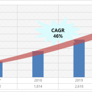
Meanwhile, according to the OLED Emitting Material Annual Report published by UBI RESEARCH, the OLED material market is expected to grow at 46% each year on average between 2016 and 2021 and record US$ 4,323 million due to the production of newcomers and the expansion of the TV OLED panel market.

161111

<OLED materials market prospect>(Source: UBI RESEARCH)

Merck-Idemitsu Kosan, OLED materials 관련 업무 협약 체결

MerckIdemitsu Kosan은 양사의 OLED materials 관련 특허권 일부를 공동 사용하는 업무 협약을 체결했다고 지난 7일 발표했다.

양사는 OLED materials을 양산하는 대표 업체로, 긴 개발 역사와 다수의 특허를 보유하고 있으며 현재 다양한 업체에 OLED materials을 공급하고 있다.

이번 협약은 긴 수명과 높은 효율을 가지는 OLED materials 개발하기 위해 마련됐다.

이를 통해 양사는 명시된 조건 하에 상대 기업의 특허권 일부를 활용하여 OLED materials을 개발에서부터 제조, 판매까지 할 수 있게 됨과 동시에 고성능 OLED materials 연구개발에 집중할 수 있게 됐다.

또한, 양사는 OLED 시장을 추가 확보하기 위해 특허권의 공동 사용 범위를 확대시키는 논의를 지속적으로 할 계획임을 밝혔다.

한편, 유비산업리서치가 발간한 2016 OLED Emitting Material Annual Report에 따르면, OLED material은 후발주자들의 본격적인 양산 시작과 TV OLED panel시장의 확대로 인하여 2016년부터 2021년까지 연평균 46% 성장하여 약 US$ 4,323 million의 규모가 될 것으로 전망했다.

161111

<OLED materials 시장 전망, 출처: 유비산업리서치>


[Lighting Japan 2016] What is the Key Issue of Solution OLED Materials?

In Lighting Japan 2016 (January 13-16) conference, Sumitomo Chemical and Merck revealed recently developed soluble OLED materials performance results.


The soluble OLED materials efficiency published in this conference reached ≥ 65% of UDC’s evaporation materials; particularly, Sumitomo Chemical’s red achieved ≥ 85%, and green reached ≥ 88% of UDC’s evaporation materials efficiency. Lifetime (LT 95) results were not as good as efficiency with red’s 25% and green’s approximately 40% (average).


Sumitomo Chemical and Merck both revealed that although in terms of efficiency the soluble materials almost caught up to evaporation materials, but lifetime requires further development.


Solution process is a method that allows for large area OLED panel production in RGB method using ≥ Gen8 manufacturing equipment. Key panel companies are actively carrying out research development, and the performance of soluble OLED material is considered the biggest issue. According to Solution Process OLED Report 2015, published by UBI Research, when solution process is applied the material cost can be approximately 40% reduced compared to the current evaporation process using large area OLED panel. The timing for the solution process application to mass production is expected to be decided depending on the development speed of soluble OLED materials.


OLED Materials Performance Comparison

OLED Materials Performance Comparison

[Lighting Japan 2016] Soluble OLED material의 핵심 이슈는?

13일부터 일본 도쿄 빅사이트에서 개최된 Lighting Japan 2016 conference에서 Sumitomo Chemical과 Merck가 최근 개발된 soluble OLED material의 성능을 공개했다.

Sumitomo Chemical은 polymer 기반의 soluble OLED material을, Merck는 small molecule 기반의 soluble OLED material을 개발 중에 있다.

이번 conference에서 발표된 soluble OLED material의 효율은 UDC의 증착재료 대비 red는 65% 이상 특히 Sumitomo Chemical의 red는 85% 이상을 달성하였으며, green은 UDC의 증착재료 대비 88% 이상의 효율을 달성한 것으로 나타났다. 수명은 LT 95에서 red는 25%, green은 약 40%(평균수치) 수준으로 효율에 비해 부족하게 나타났다.

Sumitomo Chemical과 Merck에서 말하는 공통적인 이슈는 LT 95 확보로 효율측면에서는 증착재료를 많이 따라잡았지만 수명에서 개발이 더 필요하다고 밝혔다.

Solution process는 Gen8 이상의 장비에서 대면적 OLED panel을 RGB 방식으로 생산할 수 있는 공정으로서 주요 panel 업체에서 연구 개발을 적극적으로 진행 중에 있으며, soluble OLED material의 성능이 가장 큰 이슈로 뽑히고 있다. UBI Research에서 발간한 “Solution Process OLED Report 2015”에 따르면 solution process 적용시 증착 process보다 material cost를 현재의 대면적 OLED panel보다 약 40% 절감할 수 있다고 분석하고 있으며 soluble OLED material의 개발 속도에 따라 solution process 공정이 양산에 적용되는 시기가 결정될 것으로 전망된다.

OLED 재료 성능 비교표

[Merck Display Insight 2015] Merck Reveals Latest Performance Results for Red and Green Solution Process Materials

On November 5, during the 16th Merck Display Insight 2015 seminar, Merck revealed the development results for solution process materials. The solution process materials presented were red and blue materials’ efficiency, lifetime, and CIE.


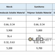
At present UDC’s evaporation materials are being used in OLED mass production. UDC’s evaporation material performance, published on the company website, were compared with Merck’s materials. Merck’s red material’s efficiency was 19.1cd/A, lifetime was 5,900 hours, and the CIE was (0.66, 0.34) which were approximately 66% of UDC material’s efficiency (29cd/A), 26% of UDC material’s lifetime (23,000 hours), and showed equal CIE.


For Merck’s green material, efficiency was 76.4cd/A, lifetime was 5,200 hours, and the CIE was (0.32, 0.63). These were approximately 89% of UDC’s green’s 85cd/A of efficiency, and 29% of 18,000 hours of lifetime. The CIE were similar with UDC’s (0.31, 0.63).


The comparison of the published materials’ performance, efficiency of solution process materials are developed to the similar levels as evaporation materials, but material lifetime require more research. Through this seminar, Merck revealed that the LT95’s solution process material’s lifetime will be solution process OLED’s most crucial challenge.


During the question and answer part of the poster session, Merck also revealed positive outlook that full stack solution process OLED product will be produced within the next 3-4 years.


Despite being one of the latecomers within the OLED material business, Merck is producing notable results in solution process material development and OLED material sales. This year’s sales results are anticipated to be higher than expected.


According to 2015 Solution Process OLED Annual Report, published by UBI Research, the key issue for solution process OLED is solution process emitting material performance. The solution process red and green’s efficiency reached to the similar levels as evaporation material. However, lifetime showed to be ≤approx. 30% of evaporation material in LT95. On the other hand, solution process blue is analyzed to be falling behind evaporation material in both lifetime and efficiency. As such, it is estimated that solution process OLED will be mass produced using the hybrid structure where red and green are formed through printing, and blue is formed through evaporation.

[Merck Display Insight 2015] Merck, soluble red, green 재료의 최신 성능 공개

Merck는 11월 5일 개최된 제 16회 Merck Display Insight 2015 세미나에서 soluble 재료의 개발성과를 공개했다.  발표한 soluble 재료는 red와 blue재료로, Merck는 이번 세미나에서 재료의 효율과 수명, 색좌표를 공개하였다.


현재 OLED 양산에는 UDC의 증착재료가 적용 중이며 홈페이지에 공개된 UDC의 증착재료 성능과 비교했을 때, Merck가 공개한 red 재료의 효율은 19.1cd/A, 수명은 5,900시간, 색좌표는 (0.66, 0.34)로 UDC 재료의 효율 29cd/A의 약 66%, 수명 23,000시간의 약 26%의 성능을 보였으며 색좌표는 동일했다.


Merck가 공개한 green 재료의 효율은 76.4cd/A, 수명은 5,200시간, 색좌표는 (0.32, 0.63)로 UDC의 증착재료 green의 효율 85cd/A의 약 89%, 수명 18,000시간의 약 29%의 성능을 보였으며 색좌표는 UDC 증착재료의 (0.31, 0.63)와 흡사했다.


공개된 재료들의 성능을 분석해보았을 때 효율은 증착 재료와 거의 근접한 수준까지 개발된 것으로 분석되지만 soluble 재료 수명은 개발이 필요할 것으로 보인다. Merck는 세미나를 통해 LT95에서 soluble 재료의 수명이 solution process OLED의 가장 핵심적인 도전이 될 것이라고 밝혔다.


또한, 포스터 세션에서 이루어진 질의 응답 시간에서는 3~4년내 full stack solution process OLED 제품 생산이 이루어질 것이라는 긍정적인 의견을 내비쳤다.


Merck는 OLED 재료 사업에서 현재 후발주자이지만 솔루션 재료 개발과 양산에 적용되는 OLED 재료의 판매에서 눈에 띄는 성과를 내고 있으며 올해 판매실적이 예상치를 뛰어넘을 것으로 기대되고 있다.


유비산업리서치에서 발간한 ‘2015 Solution Process OLED Annual Report’에 따르면 solution process OLED에서 가장 이슈가 되고 있는 부분은 soluble 발광재료의 성능으로, soluble Red와 green의 효율은 증착 재료와 거의 근접한 수준까지 개발된 것으로 나타났으나 수명은 LT95에서 증착재료의 약 30%이하의 수준으로 나타났다. 반면 soluble blue는 수명과 효율 모두 증착재료에 비해 부족한 것으로 분석되었기 때문에 solution process OLED는 red와 green은 printing 공정으로 형성하고 blue는 증착공정으로 형성하는 hybrid 구조로 첫 양산을 할 수 있을 것으로 전망된다.

Solution Process Panel, Cheaper To Produce than LCD

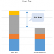
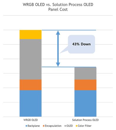
According to 2015 Solution Process OLED Report, published by UBI Research on October 14, solution process technology could produce 55inch OLED panel at approximately 43% cheaper cost compared to WRGB method.


The report added that this value is the result of analysis of 2015 Q2 55inch UHD OLED panel price and yield, which is slightly higher than current production price of 55inch UHD LCD panel. However, considering that the solution process OLED structure will become simplified and that yield of backplane and encapsulation can be improved, the OLED panels will be able to be produced at lower cost than LCD panel. The report also revealed that solution process OLED can be an alternative solution for large area OLED panel in achieving price competitiveness.


Solution process is a technology that can produce large area RGB pixel OLED panel using Gen8, or higher, equipment without cutting the mother glass. Key AMOLED panel companies are active in developing this technology.


However, as solvent is used in order to turn the existing evaporation material into ink, its purity is decreased leading to lower emitting efficiency and therefore lower lifetime. Despite these factors, key panel companies’ enthusiasm for solution process technology is due to the high emitting material usage efficiency without using color filter, and simple structure compared to WRGB OLED panel which leads to production cost decrease.


Panasonic has been most active in developing solution process applied OLED panel, and has presented several times in CES and IFA. BOE and AUO also have revealed solution process OLED panel produced via ink-jet manufacturing equipment, and CSOT is considering solution process development. Samsung Display and LG Display, leaders of AMOLED industry, are also actively developing the technology. LG Display has adopted Gen8 ink-jet manufacturing equipment, and Samsung Display has started solution process OLED panel development with a focus on ink-jet manufacturing equipment companies.


Material and manufacturing equipment companies as well as panel companies are leading the solution process technology development and commercialization. Kateeva agreed on technology collaboration with Sumitomo Chem. while Merck did the same with Seiko Epson. DuPont recently revealed that they enlarged solution process OLED material production facilities and began operation.


Following these participation by key panel, material, and manufacturing equipment companies in solution process technology development and commercialization, it is anticipated that the solution process OLED panel market will record rapid growth.


UBI Research’s 2015 Solution Process OLED Report forecast that solution process OLED panel market will actively begin mass production from 2018 and show approximately US$ 2,329 million in 2020.


Solution process OLED panel수정2

Solution process OLED panel, LCD보다 저렴하게 제작 가능

유비산업리서치에서 14일 발간한 “2015 Solution Process OLED Report”에 따르면 “Solution process로 55inch OLED panel을 현재 양산되고 있는 WRGB 방식의 OLED panel보다 약 43% 저렴하게 제작할 수 있다.”라고 분석했다.

보고서에서는 “2015년도 2사분기 기준 55inch UHD OLED panel 가격과 수율을 기준으로 분석한 수치로서 현재 55inch UHD LCD panel의 제조 원가보다는 약간 높게 나타났다. 하지만 solution process OLED의 구조가 단순화 될 것이라는 점과 backplane과 encapsulation 수율이 개선될 수 있는 점을 고려해보면 LCD panel보다 저렴하게 제조할 수 있을 것”이라고 덧붙이며 solution process OLED가 대면적 OLED panel의 가격경쟁력을 확보할 수 있는 대안이 될 것이라고 밝혔다.

Solution process는 대면적 OLED panel을 Gen8 이상의 장비에서 원장 분할 없이 RGB pixel 구조로 제조할 수 있는 기술이며 주요 AMOLED panel 업체에서 적극적으로 개발을 진행 중에 있다.

하지만 solution process에 적용되는 발광재료는 기존 증착재료를 ink화를 시키기 위해 solvent를 섞기 때문에 증착재료보다 순도가 낮아 발광효율이 떨어지고 수명이 낮을 수 밖에 없다. 그럼에도 불구하고 solution process를 주요 panel 업체들에서 적극적으로 개발하고 있는 이유는 color filter를 사용하지 않고 발광재료 사용효율이 높으며 WRGB방식의 OLED panel에 비해 구조가 단순하기 때문에 원가절감을 할 수 있다는 점이다.

Solution process를 적용한 OLED panel은 Panasonic에서 가장 적극적으로 개발을 진행해왔으며 CES와 IFA에서 여러 차례 공개한 적이 있다. BOE와 AUO도 ink-jet 장비를 이용한 solution process OLED panel을 공개한 바 있으며 CSOT에서도 기술개발 방향을 solution process로 검토 중에 있다. AMOLED 산업의 선두주자인 Samsung Display와 LG Display에서도 적극적으로 개발을 진행 중이다. LG Display는 Gen8 ink-jet 장비를 도입하였으며 Samsung Display도 ink-jet 장비업체들을 중심으로 solution process OLED panel 개발에 본격적으로 착수한 상태이다.

Panel 업체뿐만 아니라 재료와 장비업체들도 solution process 기술개발과 상용화에 앞장서고 있다. Kateeva와 Sumitomo Chem., Merck와 Seiko Epson은 기술 협업을 맺었으며 DuPont는 soluble OLED 재료 생산시설 규모를 늘리고 가동을 시작했다고 최근 밝힌 바 있다.

이처럼 solution process 기술 개발과 상용화에 panel 업체뿐만 아니라 주요 재료, 장비업체들이 참여함에 따라 solution process OLED panel 시장은 빠른 시일 내에 성장할 것으로 기대된다.

“2015 Solution Process OLED Report”에서는 solution process OLED panel 시장이 2018년부터 본격적으로 양산되기 시작하여 2020년 약 US$ 2,329 million 규모로 성장할 것으로 전망했다.

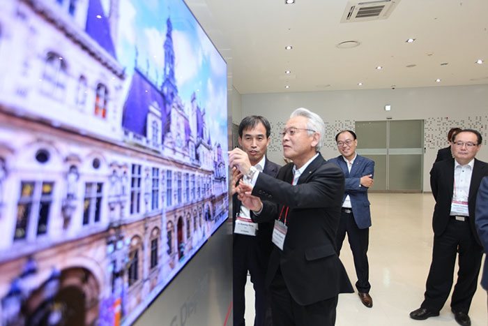
LG Display Opens 2015 Tech Forum in Collaboration with Other Companies

출처 : LG디스플레이

Source : LG Display


LG Display set out to discover new technology through open innovation in collaboration with other companies.


On September 15, LG Display invited top global display material and component companies to Paju factory and opened 2015 LG Display Tech Forum. The invited companies included Merck, Asahi Glass, and Sumitomo.


Under the heading of ‘OLED, New Opportunity and Challenge’, 13 key collaborating companies in material, process, glass, and circuitry sectors participated. They promised to share market trend, and LG Display’s OLED and LCD technology development direction and cooperate regarding future technology.


LG Display increased emphasis on OLED; LG Display revealed detailed business strategy for large and small size OLED, and discussed technology and products that should be developed together in collaboration with companies in each stage.


Additionally, LG Display newly established Technology Innovation Award for collaborating companies that contributed to LG Display’s product improvement with innovative technology. The award was presented to Asahi Glass for developing glass light guide panel used in thin panel actualization, and display material companies Merck and Nitto Denko.


LG Display’s CEO Han Sang-beom explained that LG Display could pave the way for OLED with world’s first technology due to much effort and enthusiastic corporation from R&D partners. He also entreated each company to continue to change and evolve through their own R&D competitiveness and creativity and lead the future display market.

LG디스플레이, 협력사와 함께하는‘2015 테크포럼’개최

LG디스플레이가 협력사와 함께 ‘오픈 이노베이션(개방형 혁신)’을 통한 미래 신기술 발굴에 나선다.

LG디스플레이는 15일 머크(Merck), 아사히 글라스, 스미토모(Sumitomo) 등 디스플레이 소재 및 부품 각 분야에서 세계 최고의 경쟁력을 갖춘 글로벌 협력사를 파주공장에 초청해 ‘2015 LG디스플레이 테크 포럼(Tech Forum)’을 개최했다.

‘OLED, 새로운 기회와 도전’이라는 주제로 열린 이번 포럼에는 재료, 공정, 글라스, 회로 분야 13개 주요 협력사가 참여해 시장동향과 LG디스플레이의 OLED 및 LCD 기술 개발 방향을 공유하고 미래기술에 대한 변함없는 협력을 다짐했다.

특히 LG디스플레이는 이번 테크포럼에 OLED 비중을 크게 높여 대형과 소형에 따른 OLED 구체적인 사업전략을 발표하며, 각 사업 단계 별로 협력사와 함께 개발해 나가야 할 기술과 제품에 대해 논의했다.

아울러 LG디스플레이는 이번 테크포럼부터 ‘테크놀로지 이노베이션 어워드(Technology Innovation Award)’를 신설, 혁신적인 기술로 LG디스플레이의 제품 성능 향상에 기여한 협력사에게 포상했다. 이에 박형 패널 구현을 위한 글라스 도광판을 개발한 아사히 글라스를 비롯 디스플레이 소재 업체인 머크와 니또덴코가 혁신적 기술을 인정받아 수상의 영예를 안았다.

한상범 사장은 이날 테크포럼에서 “LG디스플레이가 세계 최초의 기술로 OLED 역사를 새롭게 써 갈 수 있는 것은 R&D 파트너사의 값진 노력과 적극적인 협조가 있었기 때문이다”며, “앞으로도 각 사가 갖고 있는 R&D 경쟁력과 창의성을 바탕으로 끊임없이 변화하고 발전해 미래 디스플레이 시장을 지속적으로 이끌어 가자”고 당부했다.

Portfolio Items