Posts

[IMID 2018] OLEDON, developed ‘curved plane source FMM deposition technology’ for 2250ppi AMOLED for the first time in the world

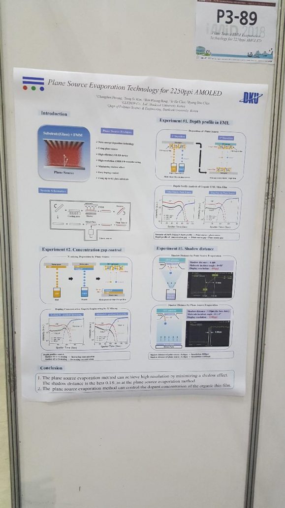
OLEDON is a company which develops plane source deposition technology for high resolution AMOLED manufacturing. Hwang Chang-Hoon, CEO of  OLEDON announced in IMID 2018 that it developed ‘curved plane source FMM deposition technology’ that can be adopted to 2250ppi AMOLED pixels, for the first time in the world.

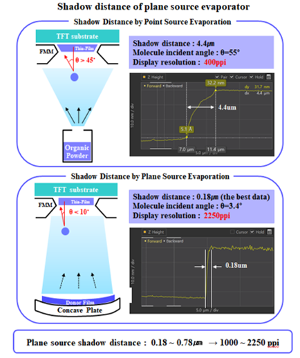
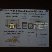
Conventional linear source FMM deposition technology has a shadow distance of 3um. The available production range is 570ppi AMOLED resolution. On the other hand, the plane source deposition technology already demonstrated in OLEDON can achieve a resolution of 800 to 1200 ppi of AMOLED with a shadow distance of 0.8 to 1.5 μm. Meanwhile, the newly developed ‘curved plane source FMM deposition technology’ is an upgraded technology of the plane source deposition technology which can realize the maximum resolution of AMOLED to 2250ppi with a shadow distance of 0.18 ~ 0.6μm.
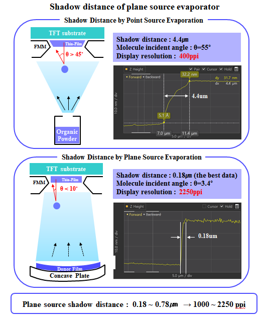
The principle is that light is gathered through a concave mirror, a curved surface is applied to the conventional flat plane source, and the light emitting material does not spread, but is precisely deposited at a desired position, thereby reducing the shadow distance.

If this technology is commercialized, it is expected that it can be widely applied not only to mobile devices but also to virtual reality devices.
[IMID 2018] OLEDON, 2250ppi AMOLED 제조용 곡면소스 FMM 증착기술 세계최초로 개발

고해상도 AMOLED 제조용 면소스 증착기술을 개발하고 있는 OLEDON의 황창훈 대표는 2250ppi AMOLED 화소의 증착이 가능한 곡면 소스 FMM 증착기술을 세계 최초로 개발하였다고 IMID 2018에서 발표했다.

기존의 리니어 소스 FMM 증착기술은 섀도우거리가 3 um으로서 생산 가능한 AMOLED의 해상도는 570ppi 수준이다. 반면, OLEDON에서 이미 선보인 바 있는 면소스 증착기술은 섀도우거리가 0.8~1.5 um 으로서 AMOLED의 해상도를 800~1200ppi까지 구현할 수 있다. 한편, 이번에 새로 개발된 곡면소스 FMM 증착기술은 섀도우거리가 0.18~0.6 um로서 AMOLED의 최대 해상도를 2250ppi까지 구현 가능한 면소스 증착기술의 업그레이드 기술이다.  

원리는 오목거울을 통해 빛을 모으는 것처럼, 기존의 평평한 면 소스에 곡면을 가해 발광재료가 퍼지지 않고 원하는 곳에 정확히 증착 되어 섀도우 거리를 줄일 수 있는 방식이다.

이 기술이 상용화 된다면 mobile 기기 뿐만 아니라 가상현실 기기 등 폭넓게 적용될 수 있을 것으로 기대를 모으고 있다.


[IMID 2017] Opening solution for next generation high-resolution OLED implementation

Various solutions for high resolution OLED implementation were released at iMiD 2017 held in COEX from October 18th to 19th. As the resolution of small and mid-sized OLEDs, which are currently being commercialized, is staying at the QHD level, the solutions released at this time have attracted a great deal of attention from display members.

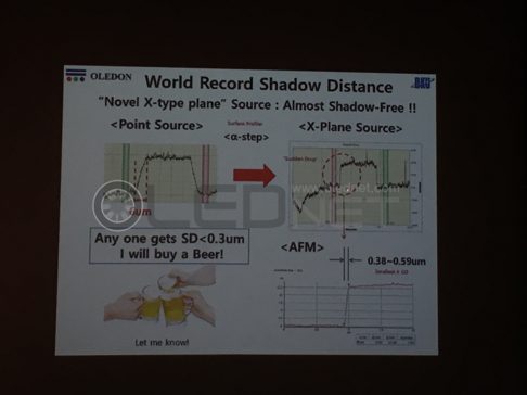
First, Hwang Chang-hoon, CEO of OLEDON, who is developing plane source FMM deposition technology, announced at the business forum, “The plane source FMM deposition technology currently being developed is the only alternative for ultra-high resolution OLED manufacturing at 2,250 ppi”. Hwang Chang-hoon CEO said, “We measured the shadow distance using a-step, and it was 0.38 μm. We can fabricate OLED device with 2,250 ppi only if we have this shadow distance.” “We are currently looking for shadow-free process conditions”

<Difference in shadow distance between point source and plane source>

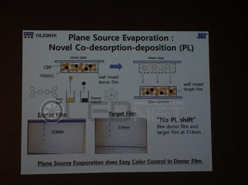
In addition, Hwang Chang-hoon said, “We first co-deposited the host material and the dopant material on the metal plate to evaporate the deposited green donor thin film and measure the green target thin film with the same PL wavelength for the first time” and “Color control of target thin films made with plate sources can be controlled by the amount of dopant molecules in the donor film, so color control is expected to be easy”.

<OLEDON plane evaporation co-deposition material>

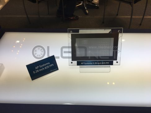
AP Systems, which recently announced the successful development of 1,000 ppi FMM using ultra-short pulse laser (USPL), exhibited 5.28 inch FMM of 825 ppi and 4.72 inch FMM of 677 ppi at this exhibition. A company official said, “By developing a burr-free laser process to solve the burr problem caused by the heat generated during the fabrication process, it is possible to fabricate not only FMM of 1170 ppi but also FMM of various shapes”.

<5.28 inch 825ppi FMM of AP Systems>

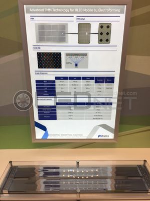
Finally, Philoptics unveiled FMMs fabricated using electro forming, especially, FMM of 1,200 ppi, which attracted attention this time, was displayed separately in the VIP room. A company official said “We have secured the stability of the process for the production of 1,200 ppi FMM,” and mentioned “We plan to deliver it to panel makers for testing in the first half of next year, and aim to develop FMM at 2,000 ppi later.”

<FMM of Philoptics manufactured by electro forming method>

As such, in this iMiD 2017, various solutions for high-resolution patterning of OLEDs has been released. Recently, as the number of contents requiring high-resolution OLED such as virtual reality contents increases, interest of smartphone users are increasingly interested. It is worth noting which solution will enable the small to medium-sized UHD OLED era.

[IMID 2017] 차세대 고해상도 OLED 구현을 위한 solution 대거 공개

지난 10월 18일부터 19일까지 코엑스에서 열린 iMiD 2017에서 고해상도 OLED 구현을 위한 다양한 solution들이 공개 됐다. 현재 상용화 되고 있는 중소형 OLED의 해상도가 QHD급에서 머물고 있는 만큼 이번에 공개 된 solution들은 디스플레이 관계자들에게 큰 주목을 받았다.

먼저, 면소스 FMM 증착 기술을 개발 중인 OLEDON의 황창훈 대표는 business forum에서 “2,250 ppi의 초고해상도 OLED 제조를 위해서는 현재 개발 중인 면소스 FMM 증착기술이 유일한 대안”이라고 발표하였다. 황창훈 대표는 “a-step을 이용하여 shadow distance를 측정한 결과 0.38 um였으며, 이러한 shadow distance를 가져야 비로소 2,250 ppi의 OLED 소자 제작이 가능하다”라며 “현재 shadow-free한 공정 조건을 찾고 있다”라고 밝혔다.

<포인트소스와 면소스의 shadow distance 차이>

또한, 황창훈 대표는 “호스트 물질과 도판트 물질을 금속면에 co-deposition하여 증착된 그린 도너박막을 재증발하여 동일한 PL 파장을 가지는 그린 타겟박막을 최초로 측정하였다”며 “면소스로 제작한 타겟박막의 칼라 제어는 도너박막의 도판트 분자의 양으로 조절이 가능하기 때문에 색 조절이 쉬울것으로 예상된다”라고 밝혔다.

<OLEDON의 면증발 co-deposition 자료>

한편, 최근 USPL(ultra-short pulse laser)을 이용하여 1,000 ppi FMM 개발에 성공했다고 발표한 AP Systems는 이번 전시회에서 825 ppi의 5.28 inch FMM와 677 ppi의 4.72 inch FMM을 전시했다. 업체관계자는 “burr-free laser process를 개발하여 제작 공정 시 발생하는 열로 인한 burr 문제를 해결하였으며, 이러한 방식으로 1170 ppi의 FMM 뿐만 아니라 다양한 형태를 갖는 FMM도 제작이 가능하다”고 언급했다.

<AP Systems의 5.28 inch 825ppi FMM>

마지막으로 Philoptics는 전해주조(electro forming)을 이용하여 제작 된 FMM들을 공개하였으며, 특히 이번에 주목받은 1,200 ppi의 FMM은 VIP room에 따로 전시하였다. 업체 관계자는 “현재 1,200 ppi FMM 제작을 위한 공정의 안정성도 확보했다”고 밝히며 “내년 상반기에 test용으로 패널 업체에 납품 예정이며 추후에 2,000 ppi 수준의 FMM을 개발하는 것이 목표”라고 언급했다.

<전해주조 방식으로 제작 된 Philoptics의 FMM>

이처럼 이번 iMiD 2017에서는 OLED의 고해상도 패터닝을 위한 다양한 solution이 공개 됐다. 최근 들어 가상현실 컨텐츠 등 고해상도 OLED가 필요한 컨텐츠들이 증가함에 따라 스마트폰 사용자들의 관심도 점점 고조되고 있다. 중소형 UHD OLED 시대는 어느 solution에 의해 개화 될지 귀추가 주목된다.