Posts

OLED deposition equipment market, who can replace Canon Tokki?

OLED-applied products continue to expand in the smartphone market. Apple plans to launch new iPhones in application of OLED technology in late 2017, and Samsung Electronics will apply OLED to its entire smartphone production. Chinese set manufacturers are employing OLED for high-end smartphones, Samsung Display’s OLED production in China is also increasing.

In response to the growing demand for smartphone OLED, major display manufacturers such as Samsung Display, LG Display, Japan Display, BOE and CSOT are currently investing or planning to invest in Gen6 flexible AMOLED mass production lines.

The size of panel manufacturers’ Gen6 flexible AMOLED mass production lines to be set for two years between 2017 ~ 2018 is approx. 20 lines based on 15K, in which the deposition equipment, one of the key equipment for OLED mass production becomes a critical element for the production facility.

Currently, Samsung Display and LG Display are the sole manufacturers of flexible AMOLED, both of which are using Canon Tokki deposition equipment. Although SNU (merged into SFA), SFA, and ULVAC have also supplied deposition equipment for the mass production sized Gen4 ~ Gen5.5 to Chinese panel makers; Sunic system supplied Gen6 deposition equipment to LG Display in 2016, yet not reaching the mass production stage. Canon Tokki is the only deposition equipment supplier for Gen6.

As a result, panel makers want to purchase Canon Tokki equipment, but unfortunately Canon Tokki’s lack of capacity for mass-producing equipment cannot entirely satisfy the panel clients’ market demand.

Consequently SFA has taken over the SNU, securing a competitiveness of deposition equipment, and succeeded in winning the deposition equipment supply contract for the Gen5.5 mass production line at GVO and Royole in China. Sunic system also received additional deposition equipment order for Gen6 in the second half of 2016, and Applied Materials is also under development to supply deposition equipment to panel makers.

In summary, the deposition equipment market originally dominated by Canon Tokki continues to be challenged by new market players. It will be a great impact to the deposition equipment market if the new market players from the panel manufacturing industry can succeed in mass production with the deposition equipment supplied by new manufacturers.
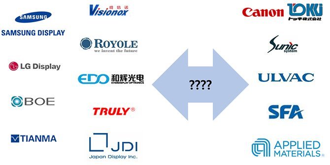
<Panel manufacturers (left) and OLED deposition equipment manufacturers (right) producing or planning to produce OLED>

OLED 증착장비 시장, Canon Tokki를 대체할 수 있는 후보는?

스마트폰 시장에서 OLED가 적용된 제품 비중이 지속적으로 확대되고 있다. Apple2017년 하반기 OLED를 적용한 신규 iPhone를 출시할 예정이고, 삼성전자도 모든 스마트폰 제품에 OLED를 적용할 것으로 전망된다. 중국 set 업체들도 high-end 스마트폰에 OLED를 채용하고 있으며, 삼성디스플레이의 중국향 OLED 생산량도 증가하고 있는 추세이다.

높아지고 있는 스마트폰용 OLED 수요에 대응하여 삼성디스플레이와 LG 디스플레이, Japan Display, BOE, CSOT등 주요 Display 제조업체에서 Gen6 규모의 flexible AMOLED 양산라인에 대한 투자를 진행중이거나 계획하고 있다.

2017~2018 2년동안 예상되는 panel 업체들의 Gen6 flexible AMOLED 양산라인 규모는 15K 기준 약 20개 라인으로 OLED 양산라인에서 핵심장비중 하나인 증착장비 확보가 이슈가 되고있다.

현재 flexible AMOLED를 양산하고 있는 업체는 Samsung Display LG Display가 유일하며 두업체 모두 Canon Tokki의 증착장비로 양산중에 있다. SNU(SFA에 합병됨)SFA, ULVAC 에서도 중국 panel 업체에 양산용 증착장비를 공급한 이력이 있지만 Gen4~Gen5.5 규모이며, Sunic system 2016년에 LG DisplayGen6용 증착장비를 납품하였지만 아직 양산단계에는 이르지 못했다. 따라서 Gen6용 증착장비를 양산한 업체는 Canon Tokki가 유일하다.

이로 인하여 panel 업체들에서도 Canon Tokki의 증착기 구매를 희망하지만 Canon Tokki의 증착장비 양산 capa가 부족하기 때문에 모든 panel 업체들의 요구를 들어 줄 수 없는 상황이다.

이에 SFASNU를 인수하며 증착장비에 대한 경쟁력을 확보하였으며 중국의 GVO RoyoleGen5.5 양산라인용 증착장비 수주에 성공하였다. Sunic system 2016년 하반기에 추가 Gen6용 증착장비를 수주하였으며, Applied Materials에서도 증착장비를 panel업체에 납품하기 위해 개발 중에 있다.

이처럼 Canon Tokki가 선점하고 있는 증착장비 시장에 후발 증착장비 제조업체들의 도전이 계속 되고있다. Canon Tokki에서도 순차적으로 증착장비 양산 capa.를 늘릴 것으로 전망되는 가운데 후발 증착장비 제조업체들이 공급한 증착장비로 panel 업체들이 양산에 성공할 수 있는지 여부가 앞으로의 증착장비 시장에 큰 영향을 미칠 전망이다.

<OLED를 양산 또는 양산 예정인 panel 업체(좌)와 OLED 증착장비 업체(우)>


Sunic System’s Successful Demonstration of 1.1um Shadow Distance, High resolution up to 1500 ppi

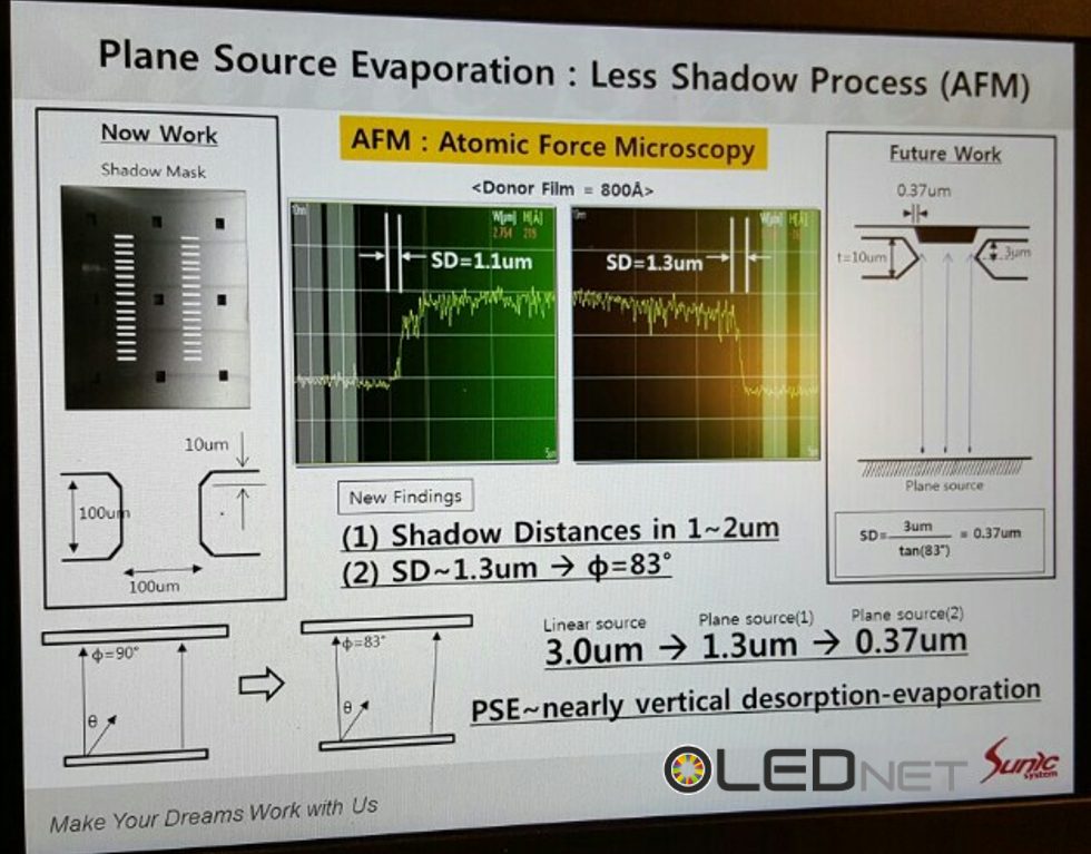
Sunic System announced at 2016 IMID Business Forum that it succeeded in implementing 1.1um shadow distance by using plane source evaporation and 100um shadow mask. 1.1um shadow distance is able to manufacture 1000ppi~1500ppi high resolution.

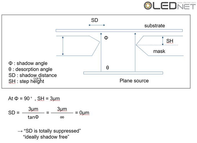
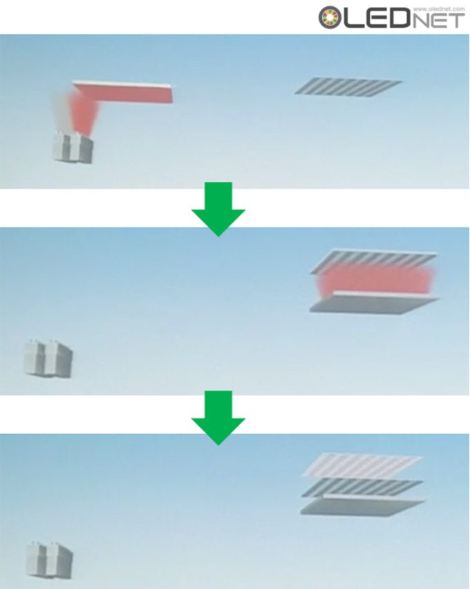
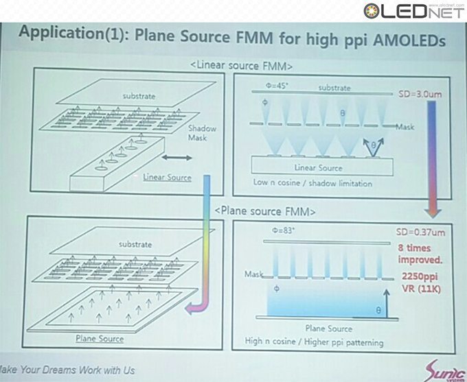
Plane source evaporation is a technology to evaporate OLED light-emitting material on metal plate, invert it, apply heat to the metal plate, and vertically evaporate OLED light-emitting material. When the shadow angle(Ф) of OLED light-emitting material evaporation is 90 degrees, the value of SD(Shadow distance, step height / tanФ) is zero (0) theoretically. So, it is possible to design thick and high resolution FMM, which means high-resolution AMOLED panel can be manufactured. This principle was announced for the first time at IMID 2016 Business Forum, attracting big attention.

Sunic System Dr. Hwang Chang-hoon said “If we lower step height up to 3um by reducing the thickness of shadow mask based on this result, 0.37um shadow distance would be possible, which means we can manufacture maximum 2250ppi(11K) high resolution AMOLED panel. Accordingly, we will put spurs to development of 0.37 shadow distance”.

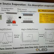
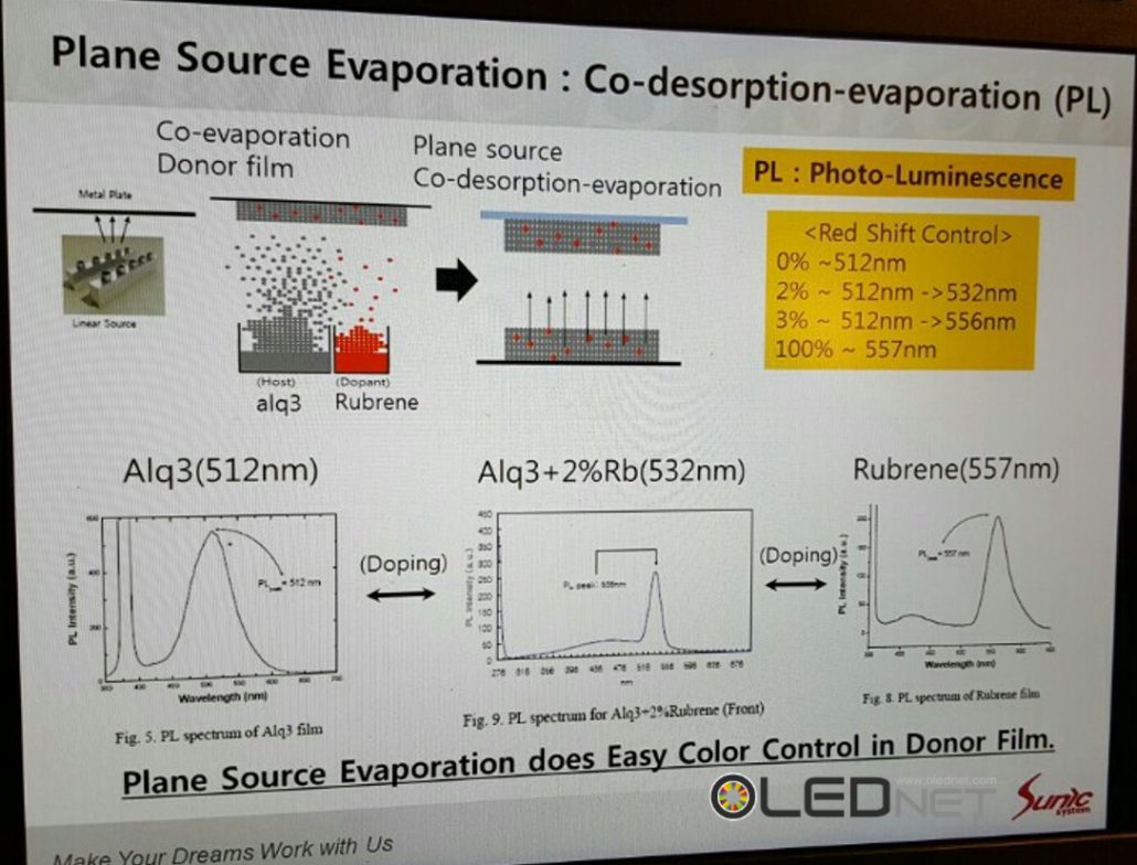
Also, he announced that co-evaporation of host and dopant that had been thought to be impossible in plane source has been resolved using flashing evaporation. He also proved that if donor film goes through flashing evaporation after co-evaporation of host and dopant, host and dopant can co-evaporate, and color control becomes easier by controlling dopant ratio to manufacture donor film.

1611021

<Result of Color Control after applying Flashing Evaporation>

1611022

<Result of 1.1um Shadow Distance>

Sunic System Suggests High Resolution 11K AMOLED Panel Solution through Plane Source

Sunic System’s solution for 11K (2,250 ppi) AMOLED production revealed in IMID 2016 held in Jeju ICC, South Korea is receiving much attention.

In the 2nd OLED Korea Conference held earlier this year, Samsung Display’s principal engineer Insun Hwang told the attendees that high resolution is the key in VR, and approximately 2,000 ppi is required for suitable realism. He explained that the resolution of VR falls as the distance between the user and display is short and this is an issue that needs to be solved.

The highest resolution of the current AMOLED panel for mobile device is 806 ppi, revealed by Samsung Display in SID 2016. The technology being applied to AMOLED panel mass production is evaporating OLED emitting materials through heat from linear source, and depositing the OLED emitting materials onto substrate through fine metal mask (FMM).

However, during the deposition stage of the OLED emitting materials, due to the distance between the evaporation source and FMM, thickness of FMM, and distance between FMM and substrate, incidence angle (θ) is produced. Due to the incidence angle, shadow distance (SD) is generated. Because of the SD issues, mask thickness and step height that minimize SD have to be decided, and these are the main reasons for the FMM production difficulty.

Shadow Distance Principle, Sunic System IMID 2016

Plane Source Process, Sunic System IMID 2016

Plane Source Process, Sunic System IMID 2016

Plane Source Application, Sunic System IMID 2016

To solve these issues, Sunic System suggested plane source, instead of linear source, and reported that this will become a key technology for high resolution AMOLED panel. Plane source technology deposits OLED emitting materials on metal plate and vertically evaporates the materials through heat after reversing that metal plate. If OLED emitting material shadow angle (Ф) becomes 90, the SD (shadow distance, step height / tanФ) theoretically becomes 0. This means FMM can be designed to be thin and high resolution, allowing for high resolution AMOLED panel production.

Sunic System’s Dr. Chang Hun Hwang explained that plane source can reduce SD figure up to approximately 8 times compared to existing technology, and 11K (2250 ppi) AMOLED panel for VR use becomes possible. Through this 8K (200 ppi) RGB OLED TV panel production becomes possible in large area SMS evaporation technology.

Particularly, if plane source using SMS evaporation technology can be applied to large area, it is also expected to have significant impact on large area OLED panel production technology.

So far, inkjet printing technology applied solution process method has been mainly developed for RGB large area OLED panel production, but soluble OLED emitting materials’ performance fall short of existing evaporation OLED emitting materials. However, if plane source technology is successfully developed and applied, evaporation OLED emitting materials can be used. Accordingly, this could become large size OLED panel production technology that replaces solution process OLED.

Sunic System supplied Gen6 evaporator to LG Display, a first for a Korean manufacturing equipment company, and active mass production is expected to be possible from 2018.

선익시스템, plane source기술로 고해상도 11K AMOLED panel 해법 제시

제주도 ICC 컨벤션 센터에서 열린 IMID2016에서 선익시스템의 11K(2250 ppi) AMOLED 제조를 위한 솔루션이 화제가 되고 있다.

올해 초 개최된 제 2회 OLED Korea Conference에서 삼성디스플레이의 황인선 수석연구원은 “VR에서는 고해상도가 핵심이며 약 2000ppi 정도 되어야 VR 디바이스에서 현장감을 잘 느낄 수 있을 것’이라고 발표하며, VR에서는 디스플레이를 접하는 거리가 가깝기 때문에 해상도가 떨어진다는 점을 해결해야할 과제로 꼽았다.

하지만 현재 mobile 기기용 AMOLED panel의 최고 해상도는 삼성디스플레이가 SID2016에서 공개한 806 ppi가 최고 해상도이다.

현재 AMOLED panel 양산에 적용중인 기술은 선형소스에서 OLED 발광재료를 열로 증발시키고 증발된 OLED 발광재료가 FMM(fine metal mask)를 통과하여 기판에 증착되는 원리이다.

하지만 OLED 발광재료의 증착과정에서 증착 소스와 FMM 사이의 거리와 FMM의 두께, FMM과 기판 사이의 거리로 인하여 OLED 발광재료가 FMM을 통과할 시 입사각(θ)이 생기게 되며, 입사각으로 인하여 SD(shadow distance)가 발생하게 된다. SD이슈로 인해 FMM을 설계시 SD를 최소화 하는 mask의 두께와 step hight를 결정해야 하며 이는 고해상도 FMM 제조를 어렵게 하는 주요 원인이다.

Shadow distance 원리, 선익시스템 IMID2016

Plane Source Process, 선익시스템 IMID2016

Plane source의 적용 application, 선익시스템 IMID2016

Plane source의 적용 application, 선익시스템 IMID2016

선익시스템에서는 이러한 문제점을 해결하기 위해 linear source가 아닌 plane source를 제안하였으며, 이는 고해상도 AMOLED panel의 핵심 기술이 될 것으로 발표했다. Plane source기술은 metal plate에 OLED 발광재료를 증착하고 뒤집은 후 metal plate에 열을 가함으로써 OLED 발광재료를 수직으로 증착시키는 기술이다. OLED 발광재료 shadow angle(Ф)이 90도가 되면 이론적으로 SD(Shadow distance, step hight / tanФ) 값이 0이 되기 때문에 FMM의 두께를 얇고 고해상도로 설계할 수 있어 고해상도 AMOLED panel 제조가 가능해 진다.

 선익시스템의 황창훈 박사는 “plane source를 이용하면 SD값을 기존대비 약 8배 까지 줄일 수 있어 VR용 11K(2250 ppi) AMOLED panel 구현이 가능해지며, 대면적 SMS 증착기술에서도 8K(200 ppi) RGB OLED TV용 panel 제조가 가능해진다.”라고 설명 하였다.

특히 plane source를 적용한 SMS 증착기술이 대면적에 적용이 가능해지면, 대면적 OLED panel 제조 기술에도 큰 파장을 일으킬 수 있을 것으로 예상된다.

현재까지는 RGB 방식으로 대면적 OLED panel 제조를 위한 기술로는 inkjet printing을 적용한 solution process이 중점적으로 개발되고 있지만, soluble OLED 발광재료의 성능이 기존 증착용 OLED 발광재료보다 낮은 이슈가 있었다. 하지만 plane source 기술이 성공적으로 개발, 적용가능해 진다면, 증착용 OLED 발광재료를 그대로 사용할 수 있기 때문에 solution process OLED를 대체하는 대면적 OLED Panel제조기술이 될 수 있을 것으로 기대된다.

한편 선익시스템은 LG Display에 국내 장비업체 최초로 Gen6 증착장비를 납품하였으며, 2018년부터 본격적인 양산이 가능할 것으로 예상된다.